
Institute Will Spur 'Synergistic' Quantum, Photonics Advancements
Eindhoven Institute of Technology (TU/e) has opened the Eindhoven Hendrik Casimir Institute (EHCI), a photonics and quantum research center. The mission of EHCI is to contribute to a sustainable information society by bringing together TU/e’s core strengths in photonics and quantum technology, from materials to systems.
The focus of the institute’s scientific program will be structured around three challenges, according to the university: computational power for solving intractable problems, energy-efficient and secure communication, and ultimate precision in sensing.
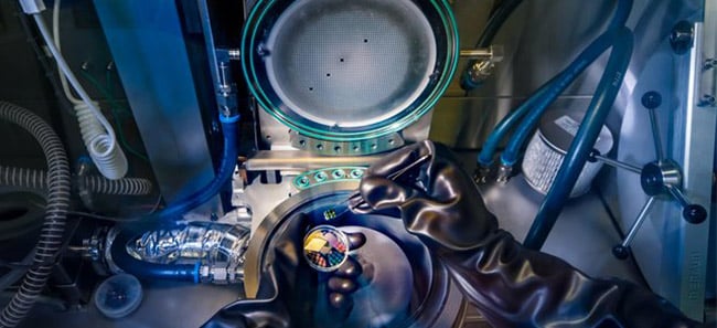
An inside look at the machine in which the nanowires that enabled silicon to emit light were grown. Courtesy of Nando Harmsen.
The university launched the center Sept. 6.
“The new institute will — unlike anywhere else in the Netherlands — smartly ‘entangle’ two major technology fields: the superfast light-driven communication technology of photonics and the mind-blowing calculation magic of quantum technology,” the university said.
Martijn Heck, scientific director of EHCI, said, “When developing new technologies, it’s all about making compromises. The new institute will bring the much-needed real synergy, in order to bring more clear directions for these fields and making the right choices.
“In 10 years’ time the institute will make significant contributions to new computing paradigms like quantum and neuromorphic computing, to novel technologies to make communication far more energy-efficient and secure and to compact biosensors for detecting diseases, and metrology sensors with atomic-scale resolution,” Heck said.
Eindhoven-based semiconductor industry supplier ASML, a TU/e partner, awarded the university €3.5 million ($4.15 million). The company said the award is to be used by researchers of EHCI. ASML said the university will also receive a ‘direct laser write lithography’ system that makes micropatterns with an ultraprecise laser beam. The device, as well as a critical dimension scanning electron microscope, will be installed in the university’s NanoLab, where it will support microchip technologies research.
The ASML gift follows multimillion dollar awards that provide support for projects and initiatives with which TU/e is involved. PhotonDelta, a European cluster of companies, knowledge institutions, and government, announced €236 million ($276.61 million) in funding in 2018 to accelerate the development of integrated photonics. TU/e then began a €17 million ($20.14 million) project under the name InPulse, to boost the production of PIC-activated products.
In April of this year, almost €1.4 billion ($1.66 billion) from the National Growth Fund (Netherlands) was set aside by the Dutch Cabinet in support of projects in which TU/e was involved — in quantum technology, green hydrogen, artificial intelligence, an integrated health care data system, and regenerative medicine.
Published: September 2021