The first integrated patterning process for next generation high-resolution devices using a nonchemically amplified metal containing photoresist and EUV lithography has been presented by nanoelectronics research center imec along with EUV photoresist developer Inpria Corp. of Corvallis, Ore., and Tokyo Electron Ltd. (TEL) of Tokyo, a semiconductor/flat panel display production equipment company.
A novel metal-oxide photoresist-based fabrication method has been demonstrated for material patterning. Courtesy of imec.
The novel metal-oxide photoresist-based method enables a significant process simplification and cost reduction compared to fab processes based on traditional organic EUV photoresists. The team transferred the metal-oxide photoresist process from the lab to the fab, demonstrating manufacturing compatibility with standard fab equipment and excellent pattern transfer capability using ASML’s EUV NXE3300 full field scanner tool and imec’s integrated process line.
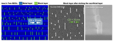
A negative tone metal-oxide EUV resist was developed by Inpria and integrated into imec’s 7-nm back end of line process module on TEL’s etching system, more specifically as a block mask layer for metal patterning with pillar dimensions as small as 21 nm. The intrinsic metal-oxide properties enabled the photoresist to also serve as a thin spin-on hard mask for the subsequent etching step.
Moreover, because of the nature of the negative tone imaging of the photoresist, further simplification in the litho-etch patterning scheme is possible, as it eliminates the tone reversal scheme required by the conventional positive tone approaches for this block patterning layer