
LEDs Offer a Lighting Makeover
New materials and manufacturing techniques are bringing LEDs closer to cost-effectiveness.
The venerable lightbulb is going high-tech, thanks to LEDs: Light-emitting diode products are more efficient, longer-lived and more versatile than incandescent and fluorescent lighting. But solid-state lighting is more expensive. Fortunately, ongoing innovations in LED semiconductors, substrates, phosphors and other materials – combined with volume manufacturing – are cutting costs, changing the value calculation in the $100 billion worldwide illumination market.
“We’re still not there yet for most of the general lighting applications, but we’re clearly approaching a tipping point,” said Eric Virey, senior analyst for LED materials and technology for Yole Développement of Lyon-Villeurbanne, France.
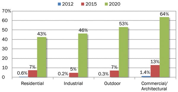
LED bulbs are rare in lamps today, but they are forecast to dominate lighting within a decade. Photo courtesy of Yole Développement.
In 2013 came several announcements of 60-W LED replacement bulbs for $10 to $15. A similarly bright incandescent bulb costs $1 or less, but an incandescent bulb outputs about 15 lumens per watt, while commercially available LED bulbs clock in at about 80. At the component level, LEDs produce about 150 lumens per watt, Virey said.
That greater efficiency favors light-emitting diodes. As a result, in applications such as display backlighting, LEDs are already present in 90 percent of shipping products, according to Virey.
Devices in the lab are approaching 250 lumens per watt at the component level; increasing performance without much added expense can slash the cost of LEDs.
Solid-state lighting consists of a photon-emitting semiconductor deposited onto a substrate. This emitter-substrate combination is then processed to create LED chips. In a device, the light produced by the semiconductor is often converted by a phosphor into a different wavelength to produce the warm white or other color desired.
In terms of lumens per watt, LED efficiency is up roughly sixfold over the past decade. There is now a slower but still impressive 15 percent year-over-year improvement.
“This is driven primarily by research in the semiconductor device itself, how the light-emitting layers are deposited, what the layers are, how the light is extracted and also development of the phosphors,” said Ted Mihopoulos, senior director of epitaxy research and development for solid-state lighting maker Philips Lumileds of San Jose, Calif.
One cost-cutting strategy is a move toward larger substrates. Philips Lumileds, like most of the industry, uses a sapphire substrate, depositing the semiconductor gallium nitride on it to create a blue-emitting LED. A few years ago, the company converted entirely to 150-mm-diameter sapphire wafers. Other manufacturers still use substrates as small as 50 mm in diameter. A larger substrate enables the use of modern semiconductor processing equipment and the handling of fewer wafers. This increases yield, productivity and throughput, thereby reducing costs.
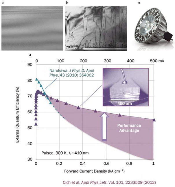 Blue-emitting gallium nitride has fewer defects on a gallium nitride substrate (a) than on the
industry-standard sapphire (b). Soraa expects to exploit this in 50-W halogen replacement lamps (c) that benefit from better LED performance. (d) GaN on GaN LED. Photo courtesy of Soraa.
Blue-emitting gallium nitride has fewer defects on a gallium nitride substrate (a) than on the
industry-standard sapphire (b). Soraa expects to exploit this in 50-W halogen replacement lamps (c) that benefit from better LED performance. (d) GaN on GaN LED. Photo courtesy of Soraa.
Sapphire is not the only substrate that can be used. LED lighting maker Cree of Durham, N.C., for instance, uses silicon carbide, but it is the only major manufacturer to do so.
Another substrate being actively investigated is silicon, as it is used to make integrated circuits. Due to Moore’s law – the doubling of device transistor count every 18 months or so – chip feature sizes steadily shrink. As a result, companies have older, underused and completely depreciated factories capable of producing thousands of wafers a week.
Buffer layers
If those factories could make LEDs on silicon wafers, they might do so very inexpensively, perhaps cutting costs in half. Some years ago, Livermore, Calif.-based Bridgelux bet this could be pulled off, according to Chief Technical Officer Steve Lester.
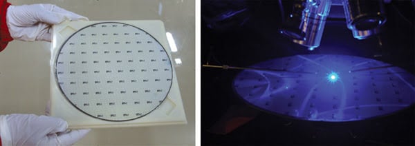
Silicon wafers such as this 8-in. (200 mm) one could be used as substrates for blue-emitting GaN LEDs, which would cut costs. Photo courtesy of BridgeLux.
The biggest challenge is the fact that silicon and gallium nitride expand at significantly different rates in response to temperature change. This thermal mismatch can lead to bowing and even cracking of the silicon wafer or gallium nitride film.
The solution is the use of buffer layers. Such layers are needed to keep the gallium from melting the silicon, but they can also play another role.
“We can engineer the flexing of the wafer during the growth in the way we desire so it ends up being flat at room temperature,” Lester said.
Besides a less expensive and larger substrate, this approach could mean that bigger chips could be built. That saves the cost of wiring many smaller chips into a single package, which is done when high luminosity is needed.
Bridgelux has managed to achieve comparable performance with its silicon substrate LEDs, Lester said. The company is sampling product and has teamed up with Japanese chip maker Toshiba to ramp the process into production on 200-mm silicon wafers. The resulting devices could appear in products soon.
Of course, the best possible match between a light-emitting layer and a substrate is when they’re the same material. Soraa of Fremont, Calif., has devised a process that creates gallium nitride on gallium nitride substrate LEDs. An advantage of this approach is that gallium nitride is optically transparent; it also is a good conductor of heat, and that brings benefits to Soraa’s devices.
“They operate at roughly 10 times the current density of standard LEDs,” said Mike Krames, chief technical officer.
Gallium nitride substrates have not been used in the past because of their cost. Soraa found a way around this, thanks to Blu-ray optical disc technology, Krames said. Blu-ray lasers require layers of gallium nitride thick enough to make a quasisubstrate. Soraa makes use of excess Blu-ray production capacity, although the company does specify its material differently.
The better performance of the gallium nitride substrate is particularly evident in replacements for high-brightness lighting products, such as 50-W-and-higher halogen lamps. More than 500 million of these were shipped this year, and Soraa hopes to do well in that market.
Other innovations are being pursued in the phosphors that transform blue or ultraviolet LED light into white color illumination. Intematix of Fremont, Calif., is a leader in this area. Coming up with the right phosphor requires engineering a material that is both pleasing to the eye and efficient, said Yi-Qun Li, the company’s chief technical officer.
It is also very important that the phosphor not change characteristics when heated from room temperature to that of boiling water. This heating happens because not all the energy going into an LED device ends up in photons going out.
“Today, most LEDs run very hot. You have 50 percent of the energy lost through the electrical-to-optical conversion,” Li said.
In general, the desire is for broad emission for green, yellow and orange phosphors, but not for red. That’s because a broad output for the last category means that some photons will be in the infrared – invisible to the eye.
One way to avoid this waste is through the use of quantum dots, according to Portland, Ore.-based Pacific Light Technologies. Standard phosphors emit over an 80- to 100-nm range, while Pacific Light Technologies’ quantum dots do so only over 30 to 35 nm, said Julian Osinski, vice president of product marketing.
The company’s proprietary methods produce quantum dot downconverters that don’t require a hermetic seal to keep out moisture. They also can withstand higher-intensity light and offer other benefits.
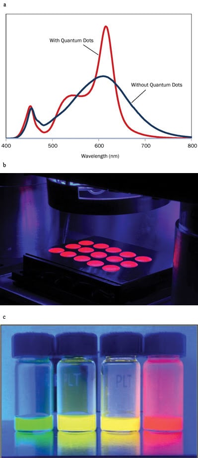
(a) White-light LED spectra made with standard phosphors (black) compared with the same with the red phosphor replaced with red-emitting quantum dots (red). Both curves give the same 3000 K color temperature, but the quantum dots are more efficient because less of the light falls outside the visible. (b) Films of quantum dots in silicon glow red in a test chamber at Pacific Light Technologies. (c) Quantum dots can be made to emit at any visible wavelength. Photo courtesy of Pacific Light Technologies.
“There’s a 30 percent or more efficiency gain,” Osinski said. “Instead of putting eight LEDs in an area lamp, you can put six in. The customer won’t know the difference, but it’ll be cheaper.”
However, the company’s quantum dots do contain cadmium, a toxin. Once encapsulated in silicone, though, the levels are below the 100 parts per million allowed by European regulations, Osinski said. He added that the company is working on a cadmium-free version and that it hopes to be in volume production of its quantum dots by 2014.
Work also is ongoing on new light-emitting materials. Silicon nanocrystals, for instance, are being researched by a team at Karlsruhe Institute of Technology in Germany and the University of Toronto in Canada. In a January Nano Letters paper, the researchers described multicolor silicon LEDs, with size-dependent emission color.
The devices have limited life spans. It also is not yet possible to produce a blue LED. But research that could fix these drawbacks is under way.
“The next step is to gain a better understanding of the degradation mechanisms of the SiLED and change the surface chemistry of the nanocrystals in order to achieve better LED performance,” said Karlsruhe graduate student Florian Maier-Flaig, adding that it will be years before any products result.
Blue and beyond
Finally, it’s important to keep in mind that there are more colors than blue. There are also red LEDs, which are constructed from indium gallium phosphide on gallium arsenide substrates. These are the subject of research aimed at improving performance and cutting costs. But at present, there are no cost-reducing alternatives to the gallium arsenide substrates, said Matthias Sabathil, director of advanced concepts and engineering at LED maker Osram Opto Semiconductors of Regensburg, Germany.
With regard to further improvements in general, the direction is up – literally. Researchers are investigating nanorods that are about a micron in diameter and 5 or 10 µm tall. Creating light-producing layers in the third dimension could substantially increase the emitting area and therefore boost efficiency.
“We are a couple of years from any product, but that’s quite promising because you can really extend the area you can use by a factor of five or 10,” Sabathil said.
Published: September 2013