After sometimes seeming like a solution
in search of a problem, lab-on-a-chip technology may be finding its footing in application-specific
incarnations, not in general-purpose devices. One key to its success is finding
the right targets and better photonics.
Helping the next generation
Josh Molho, an engineering program manager at Caliper Life Sciences
in Hopkinton, Mass., noted that lab-on-a-chip implementations originally were envisioned
as being able to replace a full-size, general-purpose lab. The combination of microfluidics,
electronics, photonics and automated processing comprising a lab on a chip promised
to shrink an entire benchtop setup into something thumbnail-size and inexpensive,
without sacrificing performance.
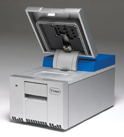
This automated nucleic acid fractionation instrument is an example
of an application-specific lab on a chip. Courtesy of Caliper Life Sciences.
Current technology does not yet match that vision – and
it’s unclear when, or if, it ever will. But integrating some functionality
is still valuable.
“It doesn’t have to be an entire lab,” Molho
said. “If, for instance, you can integrate sample preparation and analysis,
that gets you closer to a point-of-care diagnostic.”
He pointed to several recent Caliper products as illustrating
this concept of greater integration. These include new high-sensitivity glycan and
protein assay lab-on-a-chip implementations.
He also mentioned a use of the technology to improve the work
flow of next-generation gene sequencers. These devices are key to reducing the cost
of genome sequencing to less than $1000, rather than the millions needed when using
first-generation devices.
In this application, lab-on-a-chip technology automates the separation,
analysis and purification of samples going into a second-generation sequencer, a
process that today is done manually and is therefore costly, slow and prone to variation.
Caliper’s solution involves microfluidics and the use of selectively applied
voltage to isolate fragments of a desired base-pair size into a collection well.
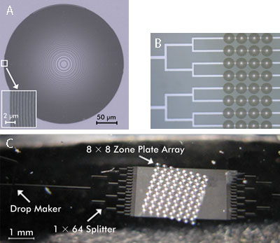
In (A), a zone plate fabricated in PDMS, a rubbery material used
extensively in microfluidic chips, allows parallel optics to interrogate parallel
channels. In (B), two microfluidic channels branch into four, then eight. Each of
the eight has four zone plates aligned to it. An implementation example can be seen
in (C), where drops travel from left to right down 64 branching microfluidic channels,
with an array of 8 x 8 zone plates providing the optics. Courtesy of Ken Crozier,
Harvard University.
Looking forward, Molho said that application-specific labs on
a chip are likely to need more powerful, better-performing, cheaper and smaller
photonics. Many of the detection schemes employed in the devices depend upon fluorescence
or make use of a variety of imaging techniques. Shrinking the optics, detectors
and light sources to a size comparable to the chip-size microfluidics is important,
particularly for something intended for handheld use.
There has been progress in this area. There are tales of the original
chip readers being too big for an elevator; current implementations fit on a bench.
Further miniaturization, however, must happen, Molho said. “You need the whole
system to get more compact.”
Photonics builds better chips
An example of how such miniaturization might be accomplished comes
from two recent research efforts. The first involves work done at Harvard University
in Cambridge, Mass. The second is from a group of companies and universities in
Europe.
At Harvard, a group led by associate professor of electrical engineering
Kenneth B. Crozier produced a solution to the measurement problem confronting many
lab-on-a-chip applications. The issue is that the microfluidics can be done in parallel
but that the detection is typically done in serial by, for instance, scanning a
focused laser spot across a chip. The result is a processing bottleneck or inferior
detection – or both.
The researchers overcame this issue, as reported in the journal
Lab on a Chip with lead author Ethan Schonbrun. They used an integrated zone plate
array, a thin silicone sheet containing embedded optics that is attached to a microfluidic
chip. The zone plate array provides the optics needed to focus excitation light
down onto a channel and the means to collect the resulting fluorescence for eventual
detection off chip.
The breakthrough lies in the parallel nature of the optics, Crozier
said. “One can excite and collect fluorescence from many microfluidic channels
simultaneously. It should be possible to scale the device up simply by fabricating
larger arrays of zone plates.”
The parallel detection capability could be useful in applications
where high throughput is needed. For other applications, this new approach offers
the advantage of an imaging system that is lighter and smaller than a traditional
microscope-based one.
In demonstrating the concept, the researchers used a 64-channel
microfluidic device with 15-μm-wide channels spaced 30 μm apart. The array
consisted of 8 x 8 zone plates, each of which achieved a high numerical aperture.
The researchers tilted these at an angle to the microfluidic channels. This arrangement
of the two-dimensional array to the one-dimensional channels allowed each zone plate
to be aligned to a unique channel.
For excitation of the resorufin dye in the demonstration, the
researchers used a 532-nm laser. They detected the resulting 575-nm fluorescence
with a high-speed CMOS camera sitting behind appropriate filters.
In a proof of concept, the researchers sent droplets down the
microfluidic channels. Their system analyzed nearly 200,000 drops per second, about
four times faster than is possible with conventional state-of-the-art methods. Crozier
said that at least a tenfold increase in throughput is possible through the use
of larger arrays of zone plates and by faster operation of the camera. There would
have to be some other changes as well, he noted. “To maintain the signal-to-noise
ratio, a higher-power laser would be needed.”
The researchers have patented their invention, and their hope
is that it will find commercial use, perhaps in something like a field assay.
Carving channels
A second example of how photonics-related innovations can play
a role in lab-on-a-chip development comes from a European research project that
ended late last year. Dubbed HIBISCUS (hybrid integrated biophotonic sensors created
by ultrafast laser systems), the project involved researchers from four companies
and two universities who used high-intensity femtosecond laser pulses to micromachine
three-dimensional features in glass microchips.
The technique created waveguides in the glass, enabling fluorescence
or other optical signals to be funneled where needed. Thus, the light from a reaction
site could be directed to a detector sitting off chip. The same technique could
be used to carve out the microfluidic channels themselves, opening up the possibility
of building chips with fewer manufacturing steps.
LioniX BV and Zebra Bioscience BV, both of Enschede, the Netherlands,
participated in the project and reportedly are developing products based on the
technique or are actively investigating its use in biochip construction. One application
could be mass production of disposable diagnostic devices.
At-home testing
A final lab-on-a-chip application-specific solution to a problem
comes from another HIBISCUS participant, the University of Twente in Enschede. Twente
graduate student Loes I. Segerink was lead author of a recent Lab on a Chip paper
that described what could eventually be an at-home fertility test. The device would
do this by counting sperm, but an extension of the idea could have other applications.
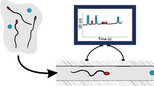
This schematic shows a lab-on-a-chip sperm detector that could be used in a home fertility test. Passing cells change the impedance of a microfluidic channel, and that can be differentiated from a polystyrene ball (cells are red, balls are blue). The variable Z represents impedance, and the Y-axis charts its absolute value. Courtesy
of Loes Segerink, University of Twente.
“In our article, I showed that it is possible to count HL-60
cells as well,” Segerink said. She added that similar schemes have been shown
by others in the past to be able to detect red blood cells and phytoplankton.
The Twente approach depends upon detecting slight changes in electrical
characteristics that arise as a result of cells traveling through a microfluidic
channel. The fluid within the channel completes a circuit. The existence of cells
changes the channel’s impedance, its resistance to alternating current.
In demonstrating their concept, the researchers built a chip out
of two glass wafers, with a microfluidic channel between them. They also constructed
platinum electrodes on one side of the channel and used these to make electrical
measurements.
Tests showed that the device could count sperm and distinguish
between them and 6-μm-diameter polystyrene beads, which are of a similar size.
Other studies showed that the device could differentiate between sperm and white
blood, or HL-60, cells that measure up to 15 μm. Finally, tests showed that
the device could measure sperm concentration, a critical parameter in assessing
male fertility.
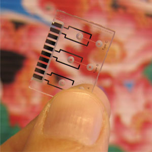
The chip in the middle, Type B, demonstrated what could form the
basis for an at-home male fertility test. Each lab-on-a-chip type consists of an
inlet and an outlet, with a microchannel in between. Electrodes located on the tapering
part of the channel are used for sperm-cell detection. Courtesy of Loes Segerink,
University of Twente.
Asked why the researchers chose to use electrical rather than
optical detection, Segerink noted group expertise in that area. She added another
reason, however, one that shows that an optical approach is not always the best.
Because no fluorescent labeling would be involved with an electrical method, there
would be no need for additional handling of the sample before a test could be done.
Less handling is better because of where the device will be used
and of who will be using it, Segerink said. “The idea is to use our system
eventually at home.”