These image sensors excel at capturing the maximum image data over the largest area possible. But they come with caveats.
JOSÉ ÁNGEL SEGOVIA DE LA TORRE, TELEDYNE E2V, AND MATTHEW KÖSE-DUNN, TELEDYNE PHOTOMETRICS
Sensor manufacturers have continuously sought to increase the resolution and performance of their products by decreasing the size of pixels while increasing their number. However, some applications require the scale and unique architecture of larger-format sensors to capture images under challenging conditions.
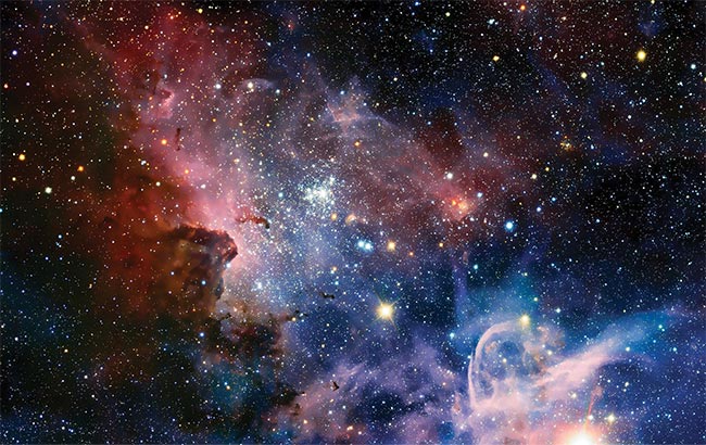
Large-format imagers incorporating large pixels (i.e., >10 µm) are typically reserved for astronomy and other applications where there is a substantial difference in illumination across pixels, or where sensitivity is a key application parameter that can only be achieved with large pixels. Courtesy of Teledyne.
Typically used for applications such as astronomy, in vivo imaging, x-ray, and microscopy, large-format sensors incorporating large pixels are required in applications where there is a substantial difference in the illumination across pixels, or where sensitivity is a key application parameter that can only be achieved with large pixels — “large” being defined here as having dimensions >10 µm.
CCD or CMOS
A long-standing debate in the machine vision industry revolves around the comparative merits of CCD versus CMOS image sensors. In the past, CCD sensors were considered superior to CMOS for high-quality imaging. However, driven by the huge amount of investment in CMOS sensors for cellphone cameras, CMOS has now become the dominant technology. In fact, Sony discontinued its CCD production in 2015 and will end support for CCDs in 2026.
Yet, CCD sensors continue to be advantageous in certain applications, such as spectroscopy, where they offer high quantum efficiency and low dark current — making them one of the best options when longer exposure times are needed. However, CCD sensors typically have a slow readout time and higher read noise, limiting their use for applications that require high-speed imaging or single-molecule levels of sensitivity. CMOS technology has also advanced to match the high quantum efficiency of CCD sensors, while offering comparable dark current. The complexity of CMOS technology previously made it harder to scale to larger formats, but improvements to the technology have overcome this drawback.
Large-format sensors present their
own twist on the CMOS versus CCD discussion. Many of the light-starved
applications in which large sensors are used require the sensor to be cooled to reduce dark current during long exposure times. Thermal management of these large-dimension sensors, and particularly CMOS chips, is difficult, making CCDs appear better suited to applications that require longer exposure times.
Many advancements have been
made during the last few years toward
developing large-format low-noise
CMOS image sensors with low-power acquisition modes. This technology
offers the possibility to dramatically reduce power consumption for long exposure modes, reducing the dark current accordingly.
In addition, new techniques have been developed to mitigate the glow effect in large CMOS sensors. This effect can limit dark current reduction because the sensor itself is emitting small amounts of light when under active biasing conditions. Teledyne and its partners have collaborated to develop techniques to reduce dark current generation and its effects through the use of shallow trenches and aluminum layers to block the sensor-generated light.
Large-format advantages
As the world moves to make everything smaller, faster, and cheaper, why should large-format sensors find favor? What are the advantages?
Small sensors imply the use of small pixels. But such architectures do not perform well in applications where there is a substantial difference in the illumination across pixels, or where sensitivity is a key parameter that can only be achieved with large pixels. Large pixels are capable of providing higher full-well capacity, which increases dynamic range where read noise is low.
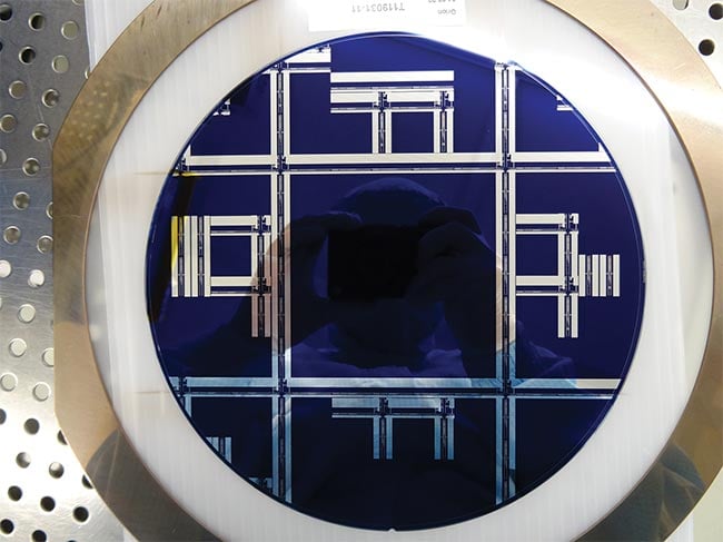
Unlike chip-scale devices, large-format imaging sensors are very sensitive to wafer-scale defects. Sensor suppliers mitigate the potential impacts of these defects by employing design-for-manufacturing rules that are even more stringent than those used by the automotive market. Courtesy of Teledyne.
Large-format imagers can perform in ways that small sensors cannot. In addition to enabling higher sensor integration, they can allow higher resolutions within a larger field of view, depending on the pixel size. This is important when imaging a large sample at high resolution, such as in microscopy, astronomy, and x-ray imaging. Sensors with a large number of pixels can also zoom in on an image while still maintaining high image quality.
Large-sensor trade-offs
Small pixel size means that fewer photons are captured per pixel. Thus, the size of pixels on a sensor directly correlates to its sensitivity. Since the area of the sensor is the square of the pixel size, even moderate changes in pixel size rapidly translate into higher or lower sensitivity. While sensitivity may not matter much for machine vision applications, where good illumination can help to compensate for lower values, sensitivity is important for sensing and scientific applications that lack active illumination.
There are, however, some drawbacks
to large-format sensors. Their cost is typically higher — even compared to using multiple smaller sensors — due to chip yield and packaging considerations.
Preclinical in vivo imaging benefits from larger sensor and pixel sizes, not only because they allow the full subject to be imaged within each frame but also because larger pixels permit the maximum amount of light to be captured. Since preclinical in vivo imaging is greatly limited by the light available, the practice requires long
imaging exposure times. Thus, large-format CCD sensors and cameras are frequently
utilized for such imaging. Courtesy of Teledyne.
Chip-scale sensors are also less sensitive to wafer defects. While a single defect on a wafer might generate a single bad device, a smaller sensor can be replaced by another sensor from the same wafer. Replacement of a wafer-scale sensor, in contrast, would require an
entirely new wafer and fabrication process. Large-format imagers also incur higher package costs because the tooling
that is required to maintain package specifications is more expensive. Further, a larger market volume exists for small sensors and packages, which typically
offers the advantages of economies of scale in terms of production costs.
The impact on integration
The size of large-format sensors does not necessarily affect integration. A high pixel count does not automatically mean
a sensor has large physical dimensions. For example, Canon’s 250-MP sensor is actually smaller in size than a common
full-frame sensor, so it can be easily integrated with existing optics or lenses. A larger sensor is often beneficial for use with the large focal planes on a telescope, or when directly imaging something without the use of optics, such as in x-ray applications.
However, the integration of large-scale sensors carries unique implications that must be considered during design.
As noted earlier, wafer-scale sensors are very sensitive to wafer defects, which makes production yields an important consideration. Teledyne DALSA and other sensor suppliers have increased the reliability of large-scale sensors by employing design-for-manufacturing (DFM) rules that are even more stringent than those used by the automotive market. Moreover, patent-protected redundant techniques are used to improve yield reliability in analog-to-digital converters and peripheral sensor circuitry.
Large-format applications
Line-scan cameras are often favored for applications such as inspecting goods on a conveyor belt, where protocols are well-defined and cost-effectiveness is a priority. Imaging tasks that need to maximize data capture over the largest area possible require large-format sensors.
Preclinical in vivo imaging, for example, benefits from larger sensor and pixel sizes, not only because they allow the full subject to be imaged within each frame but also because larger pixels permit the maximum amount of light to be captured. Since preclinical in vivo imaging is greatly limited by the light available, the practice requires long imaging exposure times. Thus, large-format CCD sensors and cameras are frequently utilized for such imaging.
In fact, the size of a large-format image sensor is highly dependent on the demands of the application. For example, electron microscopy puts a limit on sensor size. Larger sensors provide better detail, but they need to be placed farther from the microscope to allow for correct focus, imposing a logistical limit on sensor
size.
Three-dimensional (3D) stacking technology is a new alternative to expanding image sensor dimensions. It provides the possibility to integrate all of the peripheral circuitry beneath the pixel array and introduces a new opportunity to create
adjacently butted large-scale image sensors composed of multiple smaller devices. While current designs impose a dead zone of about 200 µm per side, continuing advancements will reduce this area in the coming years and allow the
development of butted devices with almost zero dead zones.
As applications for imaging technology
evolve, so do the sensors and cameras that enable these applications. Use cases ranging from gene therapy to astronomy continue to push the boundaries of large-format sensors and will lead to even greater technical advancements through research and development.
Meet the authors
José Ángel Segovia de la Torre is a senior principal engineer at Teledyne e2v, where he is responsible for the technology development of image sensors. He has authored several papers on the topic, and he contributes actively to cutting-edge sensor developments.
Matthew Köse-Dunn, Ph.D., is content
manager and applications specialist at Teledyne Photometrics. He has expertise in microscopy, life science research, and content generation. Köse-Dunn hosts Teledyne’s
“Science Off Camera” podcast.