By 2005, so-called "killer defects" may measure only 0.05 µm. The diminishing size of these flaws is driving the threshold for inspection sensitivity.
Colin Seaton, Coherent Inc.
Using optical extension techniques, ArF lasers at 193 nm already produce features as small as 0.1 μm on today’s microchips. The challenges will only increase as the industry moves to the 0.07-μm technology node by 2005.
While the number of circuits per chip continues to double every 18 months, the number of chips per wafer has quadrupled as the microelectronics industry has approached 300-mm wafer production. Meanwhile, increasing reliance on mask design and other process enhancements shortens the learning curve that chip designers must traverse to reach volume yields. Lithography sources bear only part of the burden imposed by these factors.
Lasers also provide valuable tools for inspection and measurement operations at nearly every stage of chip fabrication. Their coherent, monochromatic photons help disclose foreign matter on reticles and unpatterned wafers, as well as gauge the depth of thin films and expose errors in mask design. Leading-edge applications include the use of confocal microscopy to detect subsurface errors, holographic inspection of high-aspect-ratio vias and thin-film diagnostics based on photon-acoustic pulses. Upstream of chip production, laser-based tools help to qualify lens materials for 193- and 157-nm lithography steppers. Downstream, they help inspect features on printed circuit boards.
Although the scope and scale of laser-based metrology in the microelectronics industry are difficult to distill into a single, uniform topic, most applications, including the inspection of both reticles and wafers, adhere to certain rules in their use of lasers. Namely, lasers deliver shorter wavelengths, which correspond with the shrinking features that they both expose and detect. Higher output powers speed throughput, while laser beams with good stability and low noise help minimize detection errors.
Cost and sensitivity
The cost to open a state-of-the-art microchip fabrication plant can reach billions of dollars, with inspection equipment and processes representing a significant percentage of this. Each major process step requires one or more inspection technologies to ensure that it meets any of several manufacturing tolerances. A chip inscribed with 0.09- to 0.1-μm critical dimensions, for example, can be rendered valueless by a printed defect measuring only 70 nm. By 2005, “killer defects” may measure only 0.05 μm, and the ever-diminishing size of these flaws is driving the threshold for inspection sensitivity.
Each new generation of fabrication process increases the number of isolated process failures, which requires more defect sampling to detect and correct the failures. Also, the introduction of 300-mm wafers means that collection of process data must be performed over a larger area without incurring a throughput cost. Finally, inspection systems must be able to distinguish components with killer defects from those without. All of this drives up the cost of metrology, and because chip makers are limited as to how much they can charge per chip, they instead strive to minimize the cost of production, including measurement steps.
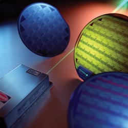
Many wafer inspection tools now operate at 488 nm. At this wavelength, solid-state lasers such as this offer more compact, efficient and low-noise alternatives to air-cooled argon-ion lasers.
Laser technology for inspecting unpatterned wafers often lags a generation behind the technology used for lithography. This means that the inspection wavelength need not be identical to the size of killer defects, particularly if those defects manifest either as foreign material on the wafer or as a raised structural flaw. Frequency-doubled argon-ion lasers at 257 nm, for example, are commonly used to detect 0.1-μm errors.
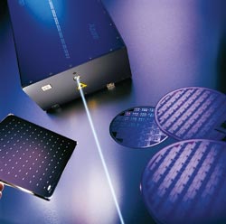
Laser technology used for inspection tends to lag a generation behind that used for lithography. State-of-the-art wafer and reticle inspection tools under development, for example, will continue to use solid-state sources at 266 nm (above) and argon-ion lasers at 257 nm.
Masks and patterned wafers present a multitude of features, many of which will scatter light. Chip makers address these light-scattering features by comparing patterned areas, either to a computer model (die to database) or to a qualified area of the same wafer (die to die). Here again, finding killer defects in masks and patterned wafers does not require the same wavelengths used for lithography applications.
The exception to this rule is aerial image mapping, which uses exposure wavelengths to detect flaws in mask design. Scattering methods may find physical flaws on a mask, but aerial image mapping simulates the exposure step to determine whether these flaws will be printed. Although accurate results are possible only at exposure wavelengths, this application doesn’t necessarily require the same type of lasers used on the production line. Many aerial image mapping instruments use compact, low-power excimers or, occasionally, solid-state sources configured to emit at exposure frequencies.
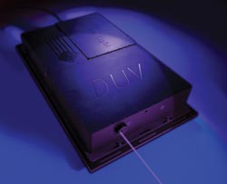
Scattering methods find physical flaws on a mask, but aerial image mapping simulates the exposure step to determine whether the mask will print these defects. Solid-state lasers provide a low-power alternative to excimer lasers for this application, which, unlike scattering techniques, must be performed at the same wavelength as lithography operations. Courtesy of Positive Light.
Whether they appear on masks or on patterned or unpatterned wafers, physical defects are exposed by the laser light that they scatter. Because smaller errors scatter smaller signals, lower-wavelength lasers provide greater sensitivity. However, increasing the output power and illuminating the wafer at shallow angles enable a longer-wavelength laser to provide adequate detection at less instrument cost.
Raising output power also maintains throughput as diffraction-limited spot sizes decrease to focus on smaller areas. But inefficiencies in harmonic conversion make higher output power problematic at these lower wavelengths. This suggests that pulsed lasers would be useful because they up-convert more easily, but inspection OEMs generally prefer to use continuous-wave sources because they provide a faster and more consistent stream of scattered signal data, which is essential to throughput.
Inspection lasers also must emit low noise. The detector must sort the signal noise from the source noise. Therefore, minimizing the laser’s noise level not only enhances sensitivity, but also shortens integration times and speeds readout.
Like lithography, inspection at any given technology node applies several generations of laser technology, with the most advanced sources performing the most advanced functions. State-of-the-art steppers this year are phasing in 157-nm F2 sources to inscribe minimum features measuring 0.1 μm. Still, ArF and KrF (248 nm) lasers will imprint features on less critical layers.
The minimum printable defect at this technology node can measure less than 70 nm. In some cases, this defect may require continuous-wave radiation in the neighborhood of 200 nm to detect. One approach is to use 244-nm radiation from a frequency-doubled argon-ion laser in a diode-pumped Nd:YAG laser cavity with a nonlinear cesium-lithium-borate crystal. This configuration provides less than 100 mW in a 198-nm continuous-wave beam.
Even the most stringent inspection applications, however, do not necessarily require this level of sophistication yet. For now, the most advanced inspection instruments rely on either diode-pumped solid-state sources at 266 nm or frequency-doubled argon-ion lasers at 257 nm. Solid-state instruments are more compact and place a lighter burden on power consumption and cooling functions. Generally, these lasers are based on Nd:YAG or Nd:vanadate technology doubled to emit at 532 nm. A resonant enhancement cavity doubles this wavelength again to produce more than 200 mW of CW output — twice that of the minimum power that previous-generation tools required for constant throughput.
Argon-ion sources continue to drive inspection applications using 488-nm light, although solid-state technology has begun competing at that wavelength. Optically pumped semiconductor lasers, however, can offer OEMs a lower-cost, more compact instrument with improved thermal characteristics and lower noise than argon-ion technology.
Patterned wafer inspection at the process research and development phase for the 100- and 70-nm nodes will require the sensitivity of scanning electron microscopy and extreme-UV instruments. But throughput requirements at these nodes yield ramp and volume production phases that will sustain demand for scattering techniques. These techniques, in turn, will sustain demand for established laser technologies.
Combining design techniques, such as double-dark-field architectures with spatial filtering, has allowed inspection OEMs to integrate longer-wavelength sources into instruments designed to inspect patterned 300-mm wafers at the 90-nm node and below. Double-dark-field architectures aim the excitation source and collect scatter at shallow angles to the wafer. This approach minimizes nonsignal noise caused by film layers that are rough or that have a high degree of color variation. More significantly, this method requires only a water-cooled argon-ion laser emitting at 364 nm.
With each new generation, inspection sources confront contradictory demands. Detecting smaller defects requires shorter-wavelength beams with smaller diffraction-limited spot sizes, but smaller defects also produce a smaller signal, requiring more intense excitation to maintain throughput.
Although harmonic conversion readily reduces wavelength, each linear crystal added to the process saps more of the fundamental wavelength’s initial power. As a rule, lower wavelengths require more powerful pumps. But this comes at a cost to footprint, power consumption and expense. There is little that laser suppliers can do to circumvent this except refine the stability of pump technology, reduce laser noise and integrate more efficient cooling systems.
Meet the author
Colin Seaton is director of marketing, semiconductor capital equipment, in the Microelectronics Corporate Business segment at Coherent Inc. in Santa Clara, Calif.
Digital Holography Hits Bottom, Returns Data
Inspection of high-aspect-ratio structures, such as contact holes or trench capacitors, poses one of the semiconductor industry’s toughest technical challenges. Scanning electron microscopes have limited penetration. Optical scattering methods used to inspect patterned wafers and masks also fall short: Although excitation photons can penetrate to the bottom of contact holes or trench capacitors, they cannot scatter out. But interferometric phase information can.
Better known as holographic measurement, phase interferometry uses diffraction patterns, not a two-dimensional image, to derive information. It creates interference patterns between two wavelengths of coherent light in phase with each other. Deriving fringes from both frequency and phase, it can ensure that a surface is flat even if that surface is at the bottom of a contact hole. Also, because a photon’s phase is directly proportional to its wavelength, phase measurements enable resolutions of one-hundredth or even one-thousandth of the excitation wavelength.
Maintaining image quality depends on factors such as exposure time, laser linewidth, and frequency, power and pointing stability. Exposure time should be minimal to speed throughput and to reduce environmental effects, such as vibration. This translates into a need for lasers with ample output power. Narrow laser linewidths and long coherence lengths are also important to contend with large path length differences as the beam scans rough surfaces. Also, a variation in laser frequency shifts the interference pattern and blurs the image. Finally, viable application of digital holography to via inspection has waited for digital video cameras that offer resolutions capable of recording the high spatial frequencies of sideband holograms.
NLine in Austin, Texas, has capitalized on evolving photonics technologies to field an instrument for direct-to-digital holography. The company recently installed a system at the Austin Sematech site for evaluation. Thus far, the technology has demonstrated inspection of the bottom of holes with aspect ratios under 12:1. The system uses a diode-pumped solid-state laser at 266 nm and a two-megapixel CCD camera. It targets the 90-nm process technology node, with an ability to identify 60-nm defects at a throughput of one wafer per hour.