Built out of fabricated elements so small as to be dimensionless, quantum dot lasers may soon have a big impact. They could, for example, help provide high-speed fiber connectivity to the home, something proponents expect shortly.
“You’re going to start seeing the deployment of these devices in the next three years,”
said Sylvain Charbonneau, applications technologies director for the microstructural
sciences institute of Canada’s Ottawa-based National Research Council.
Using light, quantum dot lasers may also link together computer
modules, and perhaps even chips, solving looming data center power problems. Beyond
that lie single-photon sources for quantum communication, as well as for potential
applications in displays and medicine.
However, reliability and cost, among other issues, have to be
navigated first. There’s also the question of competition from other technologies.
Charbonneau doesn’t consider these problems to be insurmountable.
Reliability, for example, should not be an issue, thanks to the materials and manufacturing
methods used.
Quantum dots are combinations of indium, arsenic, phosphorus and
gallium. Because they’re crystalline, under the right conditions these inorganic
semiconductors self-assemble into nanometer-size structures. Layers of such quantum
dots are produced by molecular beam epitaxy, metallorganic chemical vapor deposition
or a related technique on a semiconductor substrate, where the quantum dots act
as a lasing medium. Extensive experience has shown that this approach can produce
very reliable devices.
As for cost, quantum dot lasers offer potentially large savings.
Because quantum dots measure only nanometers, they can be thought of as dimensionless.
They therefore concentrate electrons into a ground state, resulting in emission
that is relatively temperature-insensitive; they also can be modulated quickly and
offer good noise performance.
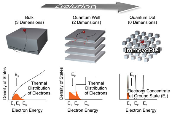
Shrinking dimensions concentrate electron states and benefit lasing.
Courtesy of QD Laser.
With quantum dots, it is also possible to create a laser with
many longitudinal modes, a consequence of the dot size dispersion. This effect has
been demonstrated by National Research Council investigators using an InAs/InP quantum
dot laser at 1.55 μm, a fiber communications standard. Some applications, such
as the wavelength division multiplexing (WDM) passive optical networks favored by
fiber-to-the-home advocates, demand multiple sources. This can be achieved economically
with a multimode quantum dot laser.
“It basically emits different laser wavelengths all at once,
addressing all of the channels in the WDM C-band or L-band or the S-band,”
Charbonneau said.
Thus, one integrated low-noise device can replace dozens of others.
That’s one reason why many companies are interested in quantum dot lasers
and why devices will appear soon, Charbonneau said.
Other quantum dot laser incarnations come courtesy of Innolume
GmbH, a startup based in Dortmund, Germany, with a US office in Santa Clara, Calif.
The company’s InAs/InGaAs quantum dot technology results in devices that lase,
depending on the recipe, from around 1200 to 1330 nm.
That happens to be critical to Raman amplification, which can
extend the reach of an optical signal. The pump lasers have to be about 80 nm below
the signal. For the upstream O-band of gigabit passive optical networks in fiber-to-the-home
applications, the pump must be 1240 nm.
Existing technologies can’t hit the required parameters,
but the new technology can, said Innolume’s managing director Guido Vogel.
“Quantum dot technology enables the building of Raman amplifiers for the O-band.”
He reported widespread interest in the approach among carriers,
and there are signs of serious consideration. For example, British Telecom researchers
Derek Nesset and Paul Wright presented a paper at the 2010 OFC/NFOEC meeting demonstrating
that, with amplification, the reach of a gigabit system could be extended to 50
km, up from about 20 km.
The wavelength could also be important to medical applications.
Fat melts at around 1200 nm, making quantum dot-based sources candidates for laser
liposuction.
When it comes to data center and, perhaps someday, chip communications,
quantum dot lasers may have a role to play. Gregory L. Wojcik, vice president of
engineering at Innolume, said the company has been working on a comb laser source
for short-reach WDM interconnects. The different quantum dot sizes lead to fairly
uniform broadband emission across low-noise nodes, each suitable for 10-Gb/s transmission.
Thanks to the resulting optical comb, a single integrated quantum dot laser can
replace dozens of discrete transmitters.
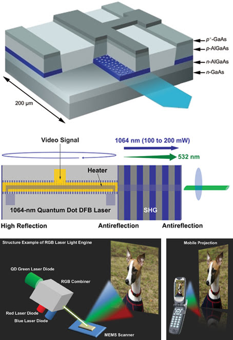
Frequency doubling (b) the output from a quantum dot laser chip (a) yields a temperature-insensitive green
source potentially useful in pico projectors and cell phones (c and d). DFB = distributed
feedback; SHG = second-harmonic generation; MEMS = microelectromechanical systems.
Courtesy of QD Laser.
Temperature is another factor to consider. Computers are hot,
and their temperature can vary over a large range. These fluctuations favor quantum
dot lasers, which offer relative temperature insensitivity. “When you start
looking at temperature, then you think that single quantum dot-based comb lasers
offer a very interesting alternative,” Wojcik said.
He added that any optical interconnect needs to break a dollar
per gigabit per second to be viable. Quantum dot laser-based solutions for short-reach
100-Gb/s optical interconnects are still several years away, but Innolume is working
to prove it can be done, he said.
Available today are products from QD Laser Inc. of Tokyo. The
company is a spinoff from Fujitsu Ltd., formed to commercialize InAs/GaAs quantum
dot laser technology developed jointly by Fujitsu and the University of Tokyo.
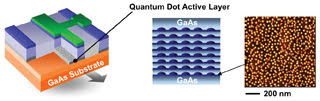
Quantum dot lasers feature an active medium containing stacked layers of high-density quantum
dots. Courtesy of Fujitsu Laboratories.
QD Laser started shipping products for the telecom market in 2010,
reported vice president of sales and marketing Michael Usami. These operate at about
1.3 μm and offer stable operation at up to 100 °C, something that isn’t
true for other lasers.
That type of performance could be useful in displays and pico
projectors, which have little or no cooling. By suitably engineering quantum dots,
QD Laser came up with a 1064-nm laser, which it frequency doubled to produce 532-nm
emission. The result is a green laser that operates at up to 60 °C, and the
company is actively working to develop markets for it. “The green laser applications
are the next challenge for us, and we expect volume production,” Usami said.
Fujitsu and the University of Tokyo continue to do research and
development in the quantum dot laser arena, announcing in May 2010 a 25-Gb/s prototype
intended for telecom applications. It is 2.5 times faster than its predecessor,
with double the density of quantum dots and 1.6 times the quantum dot layers. That
increase in the number of quantum dots by more than threefold explains the increased
data rate.
“When the number of quantum dots per unit area is increased,
the gain also rises. Furthermore, the data rate is also improved with an increased
gain,” said Yu Tanaka, a senior researcher with Fujitsu’s Atsugi, Japan-based
Nanoelectronics Research Center.
He added, though, that the relationship between the number of
dots and the data rate isn’t linear. As for the suitability of this manufacturing
approach for mass production, 50,000 laser chips can be fabricated on a single 3-in.
wafer in one batch process, Tanaka said.
Another potentially useful aspect of quantum dot lasers is that
they’re inherently radiation-resistant. This and their relatively low power
requirements make them of interest to the defense industry, said Luke Lester, professor
of electrical and computer engineering at the University of New Mexico in Albuquerque.
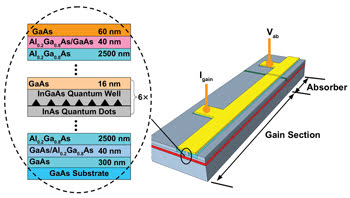
Schematic of a two-section monolithic mode-locked laser, with the quantum dot epitaxial structure
on the left. Vab = reverse bias voltage on the absorber of the mode-locked laser;
Igain = pumping current on the gain section of the mode-locked laser. Courtesy of
Luke Lester and Yan Li, University of New Mexico.
Lester’s research goal is to get to terabit-per-second
speeds at an energy cost of less than 100 femtojoules per bit. By exploiting new
technology, he believes that he has a method to get almost one-third of the way,
or greater than 300 Gb/s. “I’m looking at a single-transmitter, a quantum
dot mode-locked laser,” he said.
Further research is needed to see whether the scheme, which uses
a combination of WDM and optical time domain multiplexing, will meet the project’s
goals. Even if the technique pans out, it will be years before it results in a product.
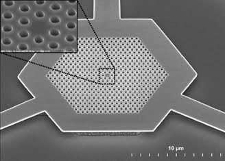
A scanning electron microscope image of an InP photonic crystal microcavity with a single missing
hole defect. Courtesy of National Research Council Canada.
Other subjects for future research and development could include
a bi-stable quantum dot laser demonstrated by a group at the National Institute
of Standards and Technology (NIST) in Boulder, Colo. The team discovered that building
a two-section quantum dot laser leads to two stable outputs with wavelengths separated
by 10 nm or so, which could be useful for wavelength switching in telecom and other
applications. Transitioning between the two states requires a short-duration voltage
pulse and is very fast, said NIST physicist Kevin Silverman. “These devices
will actually switch around the round-trip time of the cavity, so it’s basically
as fast as you can do it in a laser of that cavity length,” he said.
Schematic of a single-photon source based on a site-controlled InAs/InP quantum dot coupled to a photonic crystal
microcavity. Courtesy of National Research Council Canada.
A final future direction involves single-photon sources, which
are critical to quantum cryptography. Today, this is achieved by throttling so that,
on average, only a single photon is produced within a given time slot. However,
it would be better to have an actual single-photon source.
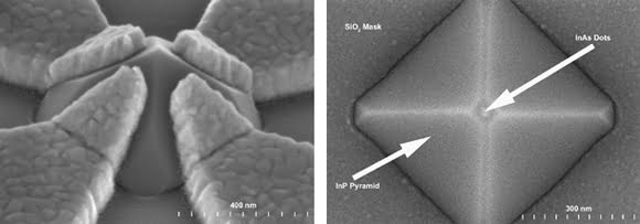
That may now be possible, thanks to a technique developed at Canada’s
National Research Council. It allows control of where quantum dots are grown on
a substrate, accomplished by lithographically opening up windows in a masking oxide
layer. Fabricating a high-Q-factor resonating cavity on top of the resulting lasing
medium leads to single-photon emitters, said the Council’s Charbonneau.
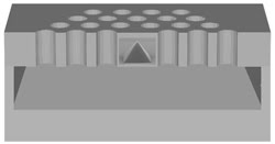
Building a single-photon source out of a quantum dot requires controlling
where the dot forms, which is accomplished by opening up a hole in a masking layer.
Courtesy of National Research Council Canada.
A great deal of research and development remains to be done before
this approach is proved feasible and production worthy, if it ever is. For that
reason, Charbonneau doesn’t see it happening soon.
Asked about a timeline for deployment, he said, “It’s five, maybe even 10 years.”