Spot-size converter laser diodes may become a vital light source for a flip-chip approach to hybrid integration of III-V-on-silicon photonics.
TER-HOE (ISAAC) LOH, DENSELIGHT SEMICONDUCTORS PTE. LTD.
The wide adoption of smartphones,
high-definition content streamed on social media, the Internet of Things, data saved to the cloud, and artificial intelligence used in massive data analytics have ushered in the current era of digital economies and Industry 4.0. These applications demand high-bandwidth optical networks and digital infrastructures capable of
massive data processing. As a result of these demands, there has been an emergence worldwide of hyperscale data centers and 5G access networks. Today, CMOS nano
electronics integrated circuits comprise the majority of information processing systems. Traditionally, optical fiber telecom networks were long-distance information carriers wherein III-V semiconductor-based optoelectronics components such as laser diodes and photodetectors were key devices in optotransceivers. The demand for high interconnect bandwidth in hyperscale data centers and access networks has brought about the replacement of copper-based system interconnects with optical interconnects.
In the past two decades, the emergence of silicon (Si) photonics has been a significant breakthrough. Information in the form of zeros and ones can be imparted into light streams through the use of
on-chip Si modulators and detected via epitaxial (epi)-grown germanium on Si. Leveraging the existing high-volume CMOS manufacturing infrastructure, Si photonic integrated circuits (PICs) are potentially low-cost and capable of high-density integration. Their drawback is that silicon is not an efficient light emitter. Laser diodes for optical fiber communications are all based on InP (indium phosphide) and its related III-V compound semiconductors. To marry the benefits of both types of semiconductors, hybrid integration of III-V-on-Si laser diodes was proposed and demonstrated as a light source for Si photonics by Alexander W. Fang and colleagues as well as by Elton Marchena and colleagues1,2.
The integration1 was done by direct bonding of a III-V epiwafer on Si prior to laser diode device fabrication. However, another approach of hybrid integration has since been demonstrated by Marchena
and others via the use of flip-chip bonding of the laser diode on a Si photonics platform wherein laser diodes and Si PICs
are separately fabricated in their respective fab prior to being mated at the back end2-5. The latter approach can be taken successfully, as it allows the integration of known-good dies of each individual fab processing and offers potentially high yield. In addition, flip-chip bonding offers the advantage of better thermal dissipation and independent optimization of III-V and Si devices.
Flip-chip approach
In the flip-chip approach, laser diodes usually operate as a continuous-wave light source and are bonded at the remote part of the Si photonics platform, which gives the least thermal crosstalk to the core of the Si photonic chip. For this type of flip-chip approach to be manufacturable, a spot-size converter (SSC) is designed into the output of the laser diode, not only to match the mode sizes of both the laser diode and the Si-PIC waveguide, but also to improve the misalignment tolerance between the laser diode output facet and the Si-PIC waveguide. To improve the coupling efficiency from laser diode to Si PIC, the far field (FF) and circular symmetry of the laser diode emission must be improved.
The general design approach taken by
the research team at DenseLight was to realize a III-V SSC capable of mode-matching the laser diode to a Si-photonic waveguide for flip-chip-based hybrid integration of III-V on Si.
An SSC laser diode (SSC-LD) is schematically shown in Figure 1. It consists of the 2-µm-wide ridge, with light generated and guided in the InGaAsP multiple (5) quantum well (MQW) active layer, linearly tapered down to a submicron-wide taper tip for adiabatic mode conversion to a middle InGaAsP-core transition waveguide (TWG). By tapering the TWG, light in the TWG further transitions to the bottom diluted waveguide (DWG). The DWG consists of several periods of InGaAsP/InP bilayers wherein a thin InGaAsP layer and a thicker InP layer give the bottom waveguide core of low-index contrast to the InP substrate beneath it.
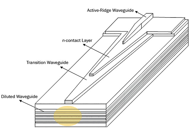
Figure 1. A 3D schematic view of an SSC. Courtesy of DenseLight.
The purpose of the low-index contrast in the diluted waveguide is to give an
output beam of a low FF angle for good
mode matching to either a single-mode fiber (SMF) or a Si PIC. Mode conversion
is done by lateral tapering of the active ridge, the n-contact, and the TWG layers. Additionally, the consecutive overlap of
the ridge, the n-contact, and the TWG
tapers along longitudinal direction give a vertical tapering effect, which results in good conversion efficiency. Conventional contact photolithography coupled with vertical sidewall etching were used to realize the structures.
The size of the mode field at the output facet of the SSC is determined by the width of the facet. For coupling to the Si PIC, the output facet width is 5~6 µm. Figure 2 shows the results for an SSC with a 10-µm-wide output facet suitable for coupling directly to an SMF. Figures 2a and 2b show the FIMMPROP simulation of
the SSC, and the mode conversion efficiency is 96%, with a calculated FWHM far
field of 9° (v) × 10.5° (h). Figures 2c-2e show the output mode, the FF, and the SEM image of the output facet, respectively.
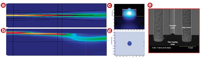
Figure 2. A FIMMPROP simulation of the SSC. Top view (a); side view (b); output facet mode profile (c); FF profile (d); and SEM image of output facet of the SSC (e). Courtesy of DenseLight.
Figure 3a shows the light power versus current (L-I) plots of 4 dies of 1550-nm-emission Fabry-Pérot laser diodes (FP-LDs) with an SSC at both ends for active laser lengths (excluding the SSC) of 960 and 1360 µm. The vertical axis refers to one-sided optical power. The threshold current ranges are 121~132 mA for an
active laser length of 960 µm, and
129~144 mA for an active laser length of 1360 µm. The average threshold current densities are 3.85 and 3.25 kA/cm2, for
active lengths of 960 and 1360 µm, respectively. The one-facet output slope efficiencies are 0.14 and 0.16 W/A, for active laser lengths of 1360 and 960 µm, respectively.
Figures 3b and 3c show the near-field mode profiles of the FP-LD at an injection current of 200 mA. This is to show that
the mode size is increased due to the SSC. Figures 3d and 3e show the FFs of the FP-LD without and with the SSC at both ends. As shown in Figure 3d, the FFs of the FP-LD without the SSC are 37.4 (v) × 24.6 (h) at full width half maximum (FWHM). This is typical of high-index contrast ridge waveguides formed by vertical sidewall etching through the MQW active layer. In comparison, the FP-LD with the
SSC has an FF of 17.5 (v) × 14.5 (h) FWHM, which shows that the FF is reduced by half with the utilization of the SSC. This experimental data confirms the effect of the SSC, although the measured FFs are larger than those by simulation because a passive waveguide without current injection was assumed in the simulation model.
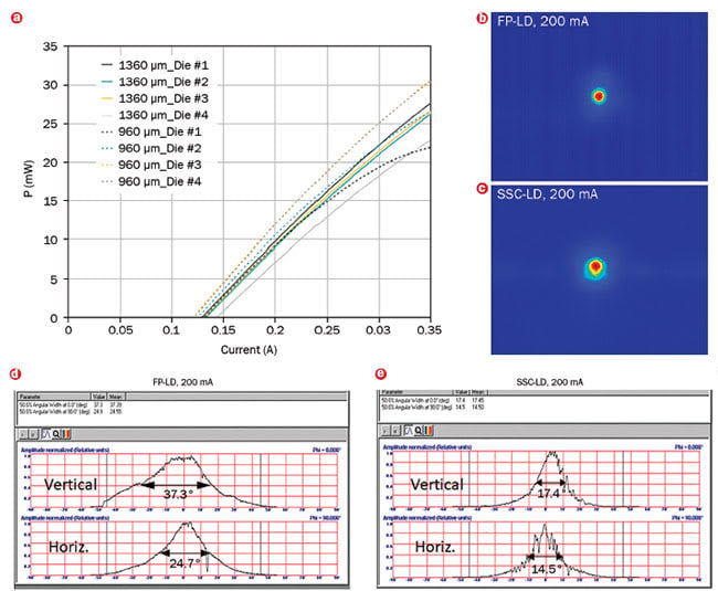
Figure 3. Light-current plots of an FP-LD with an SSC at both ends (a). Near-field mode profiles for the FP-LD without an SSC (b) and with an SSC (c). FFs measured for the FP-LD without an SSC (d) and with an SSC (e) at both ends. Courtesy of DenseLight.
In summary, the research team has designed and realized a triple-core, lateral-tapered, SSC integrated FP-LD fabricated by single epistack growth and vertical sidewall mesa etching to form lateral
tapers. The increase in mode size and a narrowing of the FF in the SSC-LD was observed compared to the FP-LD without the SSC. Such an SSC-LD formed by
single epigrowth and lateral tapering by conventional etching processes is potentially a lower-cost approach to coupling laser optical power to a Si PIC or SMF.
Meet the author
Ter-Hoe (Isaac) Loh is senior principal product development engineer for design at DenseLight Semiconductors Pte. Ltd. He has 13 years of R&D and product development experience in both III-V optoelectronics and Si photonics.
References
1. A.W. Fang et al. (2007). Hybrid silicon evanescent devices. Mater Today, Vol. 10, pp. 28-30.
2. E. Marchena et al. (2013). Integrated tunable CMOS laser for Si photonics. Presented at OFC/NFOEC, PDP5C.7.
3. Shiyun Lin et al. (2016). Efficient, tunable flip-chip integrated III-V/Si hybrid external cavity laser array. Opt Exp, Vol. 24,
p. 21454.
4. T. Matsumoto et al. (2019). Hybrid-
integration of SOA on silicon photonics platform based on flip-chip bonding.
J Lightwave Technol, Vol. 17, pp. 307-311.
5. R.A. Budd et al. (2015). Semiconductor optical amplifier packaging for scalable and gain-integrated silicon photonic switching.
Presented at Electronic Components & Technology Conference, pp. 1280-1282.