
Light Links Graphene, Gallium
BRAUNSCHWEIG, Germany, Sept. 18, 2009 – Using a light optical microscope, Physikalisch-Technische Bundesanstalt (PTB) scientists have succeeded in making graphene visible on gallium arsenide. Previously it has been possible only on silicon oxide.
Now that they are able to view the graphene layer, which is thinner than one-thousandth of a light wavelength, the researchers want to measure the electrical properties of their new material combination.
Graphene and gallium arsenide are considered top candidates for the future of electronics. Graphene is extremely thin, and its electronic properties are ideal because its electrons can move tremendously fast, making it the perfect partner for gallium arsenide, the semiconductor that allows electrical and optoelectronic components. Additionally, it is possible to produce gallium arsenide with an atomic-layer-smooth surface, which is well-suited as a support for graphene.
The normally practically invisible single-carbon-atom layers can be made visible under a normal light (optical) microscope, if the support (layer) is designed as an anti-reflection filter. Single-layer graphene was identified inside the markings.
They use the principle of the anti-reflective layer – if on a material one superimposes a very thin, nearly transparent, layer of another material, the reflectivity of the lower layer changes clearly visibly. To make their lower layer of gallium arsenide (plus graphene atomic layer) visible, the PTB physicists chose aluminum arsenide (AlAs). However, it is so similar to gallium arsenide (GaAs) in its optical properties that they had to employ a few tricks: They vapor-coated not one but rather several wafer-thin layers.
“Thus, even with optically similar materials, it is possible, in a manner of speaking, to ‘grow’ interference effects,” said Dr. Franz-Josef Ahlers, department head at PTB. “This principle is known from optical interference filters. We have adapted it for our purposes.”
First, Ahlers and his colleagues calculated the optical properties of different GaAs and AlAs layers and optimized the layer sequence such that they could expect a sufficiently good detectability of graphene. Following this recipe, they got down to action and, with the molecular beam epitaxial facility of PTB, accurately produced a corresponding GaAs/AlAs crystal atom layer. Then in the same procedure as with silicon oxide, it was overlaid with graphite fragments.
“Different from silicon but, as predicted by the calculation, although single carbon layers are no longer visible at all wavelengths of visible light, it is, however, possible, e.g., with a simple green filter, to limit the wavelength range such that the graphene is easily visible,” explained Ahlers.
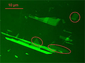
In the photo, all lighter areas of the dark GaAs are covered with graphene. From the degree of lightening, it is possible to conclude the number of individual layers of atoms. The marked areas are “real,” that is, single-layer graphene. But next to them there are also two, three and multiple layers of carbon atoms, which also have interesting properties. This arrangement was confirmed again with another method, Raman spectroscopy.
Following such a simple identification with a normal light optical microscope, the further steps in the manufacture of electrical components from graphene surfaces are now possible without any difficulty. Thus the PTB scientists can now begin to accurately measure the electrical properties of the new material combination.
For more information, visit: www.ptb.de
Published: September 2009