NAGOYA, Japan, March 10, 2021 — Researchers from Nagoya University and the Technical University of Darmstadt developed a method to quantitatively study the effect of light on nanoscale mechanical properties of thin-wafer semiconductors or any other crystalline material.
The method, which the researchers characterized as “photoindentation,” uses a tiny, pointed probe to indent the material while a light source illuminates the material in a controlled environment, in which the depth and rate at which the probe indents the surface can be measured.
The probe creates dislocations, or slippages of crystal planes, near the material surface. The researchers observed the effect of light at a range of wavelengths on dislocation nucleation (the birth of new dislocations) and dislocation mobility (the dislocations’ gliding or sliding away from the point where they were created) using a transmission electron microscope. The nucleation and mobility are measured separately, which is a distinguishing aspect of the photoindentation technique.
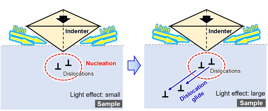
Schematic illustration of how light affects the nucleation (birth) of dislocations (slippages of crystal planes) and dislocation motion, when the sample is also placed under mechanical loading. The Nagoya University/Technical University of Darmstadt research collaboration has found clear evidence that propagation of dislocations in semiconductors is suppressed by light. The likely cause is interaction between dislocations and electrons and holes excited by the light. Courtesy of Atsutomo Nakamura, Nagoya University.
The team found that while the light has a marginal effect on the generation of dislocations under mechanical loading, the effect on the motion of dislocations is of a more noticeable significance. When a dislocation occurs, it is energetically advantageous for it to nucleate, or conjoin with others, compounding the imperfections. Electrons and holes excited in the semiconductor by the light (the “photo-excited carriers”) do not affect the strain energy of the dislocation. It is this energy that determines the “line tension” of the dislocation that controls the nucleation process.
Dislocations can, however, move in a “glide-motion.” When this happens, dislocations drag photo-excited carriers through an electrostatic interaction. The effect of photo-excited carriers on this dislocation motion is far more pronounced; if enough carriers are produced, the material becomes much stronger.
The effect is stark when the experiment is carried out in complete darkness, and then under illumination at a wavelength that matches the semiconductor bandgap to produce more photo-excited carriers. Typically, when a solid material is indented, it initially goes through a process called “plastic deformation” in which it changes shape without springing back, until the load becomes too great and the material cracks.

Conversely, the Nagoya group showed that the inorganic semiconductor zinc sulfide (ZnS) behaved more like a putty when in total darkness; it can deform by 45% under shear strain without cracking or falling apart. When illuminated by the correct wavelength, however, it becomes quite hard. The increase in hardness is less pronounced at other wavelengths at which the researchers tested.
The results show that purely plastic deformation without crack formation in semiconductor materials occurs at the nanoscale. Insofar as the results yielded information about mechanical behavior, in the context of the work semiconductors resemble metallic materials. The newly established experimental protocol makes it possible to evaluate the effect of light on the strength of even nonsemiconducting materials that are very thin.
“One particularly important aspect is that nonsemiconductors can exhibit semiconducting properties near the surface, due to oxidation, for instance, and since the starting point of deformation or fracture is often the surface, it is of great significance to establish a method for accurately measuring the strength of materials under controlled illumination conditions at the very surface, on a nanoscale,” said Atsutomo Nakamura, associate professor at Nagoya University.
Previously, the atomic structure of a material was the smallest unit of consideration when thinking about a material’s strength. In other words, the premise of strength was understood from atomic arrangement and elasticity theory. However, recent studies have indicated that the characteristics of a material’s strength take significant influence from externalities such as light and electric fields.
“It is becoming more and more accepted that other viewpoints must be added to the theory of material strength, which include the motion of electrons and holes that are smaller than atoms,” Nakamura said. “This study reaffirms the quantum-level effect on the strength of such materials. In this respect, it can be said that this research has achieved one milestone in the paradigm shift in the field of material strength that is currently occurring.”
“Now that the creation of devices on the true nanoscale is becoming a reality, the impact of light on the structural strength of various inorganic semiconductors is an issue to be considered,” said Xufei Fang, a professor at the Technical University of Darmstadt.
The research was published in ACS Nano Letters (www.doi.org/10.1021/acs.nanolett.0c04337).