With adoption into smartphone technology and lidar, VCSELs — developed in the 1980s — are being tapped for new applications.
FAROOQ AHMED, CONTRIBUTING EDITOR
By the end of 2018, nearly 1 million sq ft of new production space will have opened in the previous two years — space dedicated to making some of the world’s smallest and least power-hungry lasers. Known as vertical-cavity surface-emitting lasers, or VCSELs, these miniature devices have found use in 3D sensing, lidar, automated driving and manufacturing, high-speed data communication, laser printers, optical mice, and smartphones.
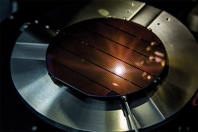
A VCSEL wafer in production.
Sunnyvale, Calif.-based Finisar recently completed a 700,000-sq-ft facility in Sherman, Texas, to produce the components. Austria-headquartered ams, which acquired N.J.-based VCSEL manufacturer Princeton Optronics last year, committed $200 million to increase production at a site in Singapore. And in late 2017, Philips Photonics, together with the European Union and Germany’s Federal Ministry of Education and Research, completed a €23 million (approximately $26 million) upgrade to its facility in Ulm, Germany, to double VCSEL production at the location. A market report from BCC Research estimates that VCSELs will be a $3.6 billion business by 20201.
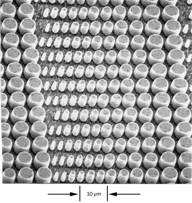
Figure 1. Close-up of a scanning electron microscope image from 1989 of a 6- × 8-mm chip with more than 1 million VCSELs. Photo by Axel Scherer.
Like many now widely used technologies, VCSELs had their start with another purpose in mind (Figure 1). Axel Scherer, a Caltech professor who developed early prototypes of the lasers at Bell Labs in the 1980s, said optical computing drove the initial research.
Integrated optics
VCSELs are multilayered devices that typically consist of active regions with sufficient quantum wells to generate laser light sandwiched between optical mirrors. A diode junction directs electric current and generates light. Molecular beam epitaxy, a manufacturing technique also developed at Bell Labs, allowed Scherer and colleague Jack Jewell to grow their new device with “very accurate thickness … controlled within about 1 percent,” Scherer said.
According to Scherer, “Integrating optics and electronics has been traditionally difficult.” However, refinements in production techniques in the past two decades have allowed VCSELs to now be manufactured lithographically, often in automated facilities, on gallium arsenide wafers for wavelengths from about 400 to 1500 nm (opening photo, left). Unlike edge-emitting lasers, VCSELs beam laser light perpendicular to their surface, which allows scores of them to be placed on a single chip without increasing the thickness of a circuit board. This also allows them to be mounted without the need for additional mirrors.
Smarter phones
Smartphone manufacturers such as Apple are capitalizing on the compact
nature of VCSEL arrays and their low power consumption for novel uses. The latest iteration of Apple’s flagship smartphone, the iPhone X, uses an IR VCSEL array for time-of-flight analysis as part of its TrueDepth module for 3D imaging. The array is in an always-on state, tracking objects that appear in front of the phone’s screen, and the information is deployed in 3D facial identification, portrait selfie photographs, and animated emojis or “Animojis.” Scherer said, “Probably every subsequent generation of not just iPhone but other phones will now start using VCSELs,” because of Apple’s adoption of the technology. Indeed, in July, ams announced that the Chinese Android phone maker Xiaomi had deployed its low-power IR VCSEL in the new Mi8 Explorer Edition smartphone (Figure 2).
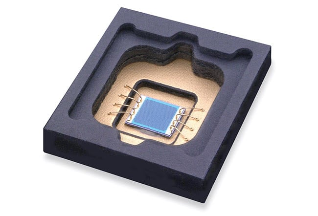
Figure 2. High-power sensor VCSEL in package.
In December 2017, Apple promised $390 million to Finisar as part of a
$1 billion commitment to U.S. manufacturing. (II-VI Inc. announced last month that it will aquire Finisar.) According to Craig Thompson, Finisar’s vice president of marketing and business development for 3D sensing, the technology has “really taken off in the last few years.” He said they have been “shipping low-powered, single-mode VCSEL sources [for] a variety of sensing applications for 10 years or more.” The investment from Apple “was the catalyst for a very high-volume mainstream adoption of our structured light sensing,” and this has “led a number of us in the laser supply chain to invest fairly heavily in the last couple of years to prepare for that surging demand. For the foreseeable future, the lion’s share of the industry volume will go into smartphones” (Figure 3).
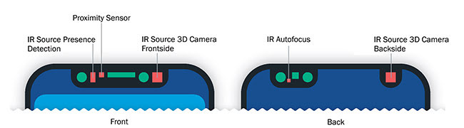
Figure 3. VCSELs in a smartphone.
Part of the appeal of VCSELs is that they can be deployed like light-emitting diodes (LEDs). “The LED was very popular early on but quickly ran into limitations around spectral bandwidth and wavelength variability,” Thompson said. “It’s a broadband light source.”
Scherer agrees that “for the same amount of power, you’re better off using a VCSEL over an LED. It’s cheaper to make.”
Finisar’s new Texas facility gives it control over VCSEL design and manufacturing from fabrication, backend processing, and testing, Thompson said. In the short term, he believes that innovations will come by achieving higher VCSEL energy efficiencies, squeezing more emitters on a single die, developing smaller light apertures to allow for more-focused beams, and “packaging innovation to make [them] easier and cheaper to deploy. There’s a lot to be learned or borrowed from the LED industry.” In the future, he thinks smartphones will “move away from just doing facial ID authentication and emojis to doing more complicated 3D mapping [and] 3D imaging, and using that information to enable true augmented reality.”
Smarter vehicles
Another rising application for the
minute lasers is in lidar and advanced driver assistance systems for the next
generation of automated vehicles. Although not widely used at this point on account of cost and physical bulkiness, lidar is making inroads.
Alphabet Inc.’s self-driving car subsidiary, Waymo, which had its origins at Google, is deploying lidar in its vehicles. (Elon Musk’s Tesla uses a combination of radar, ultrasonic sensors, and optical cameras in its vehicles’ autopilot mode — instead of lidar.)
Finisar’s Thompson said they are seeing interest in short-range flash lidar for object detection in the automotive space (Figure 4).
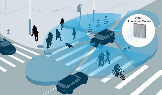
Figure 4. Lidar for 3D sensing in vehicles.
In 2016, Japanese-based Denso Corp., which is one of the world’s largest suppliers of automotive components, invested in TriLumina, an Albuquerque, N.M.-based manufacturer of VCSEL semi-
conductor lasers. TriLumina makes 940-nm, back-emitting, flip-chip VCSEL modules.
Reached by email, Luke Smithwick, the company’s chief marketing officer, said, “With this architecture, we have
excellent electrical properties as well as the ability to monolithically etch microlenses onto the frontside of the die. Each VCSEL can be individually addressed, although normally done in groups, allowing us to do true solid-state scanning.” He believes the cost and size of future lidar rigs will significantly decrease with the transition to VCSEL illumination modules.
TriLumina is working on VCSEL deployment inside the car as well. Occupant monitoring systems act as an advanced form of in-cabin, near-IR camera, enabling the vehicle to understand the positions, sizes, and activities of the driver and passengers (Figure 5).
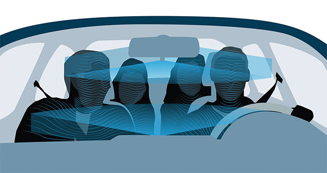
Figure 5. Lidar for in-cabin monitoring inside vehicles.
Based on time-of-flight measurements
and 3D scanning, these systems could make real-time adjustments to the vehicle’s cabin — from disabling airbags for smaller passengers to preconditioning the vehicle’s interior in the event of an accident — responding to drivers’ and passengers’ situational awareness and positioning. Smithwick said, “Historically, LEDs have filled the illumination need for occupant monitoring systems, but now 940-nm, small-footprint, low-power, low-cost VCSEL arrays are be-com-ing the illuminator of choice.” In-cabin VCSEL use in commercial vehicles, trains, and planes could also help investigators determine causation in crash investigations.
Faster optical communication
One of the earliest commercial uses for VCSELs was as links in fiber optic data transmission. According to Jack Jewell, who developed VCSELs with Scherer at Bell Labs, “The optical communication market was the first large market for VCSELs when [they] came out of the lab.” Demand for this use continues to grow with the construction of massive data centers in this “big data” era of science, with a push toward increased transmission rates. “One of the exciting developments has been the use of wavelength division multiplexing.”
Current fiber optics can operate at a
data rate of 25 Gb/s, but because of multiplexing, “there are four wavelengths each at 25 — so you’re getting 100 [Gb/s] down a single fiber,” Jewell said.
Milton Feng is the Nick Holonyak Jr. Chair Professor of Electrical and Computer Engineering at the University of Illinois at Urbana, Champaign. (In 1990, Holonyak helped developed the III-V native oxide, which is used for current and optical confinement in semiconductor lasers.)
Feng recently demonstrated that oxide-confined VCSELs have an error-free data transmission rate of 50 Gb/s at 85 °C — a temperature requirement for large data centers2. He said a new fabrication method, which they are currently patenting, has allowed them to “double the transmission rate. Multiplexing 50 Gb/s fibers would allow for 200 Gb/s transmission over 100 m.”
Transitioning to transistors
Scherer was not initially bullish on VCSEL technology. He said, “I got out
of the field [for a time] because I thought it was all done.” He’s now leveraging
VCSELs for optical communication within the body because “this gives us the ability of very large bandwidth communications and optical isolation that allows you to have less noise” when sending a signal from a biologically connected device.
Jewell sees the potential for VCSELs
to transform how we use atomic clocks (Figure 6). With portable microatomic clocks, he said, “we have far more accurate GPS,” and “it’s helped U.S. Army backpack communications a great deal because you have a clock that’s light enough to carry, including the power source, and so precise that you can code your signals in a much more complex way.”
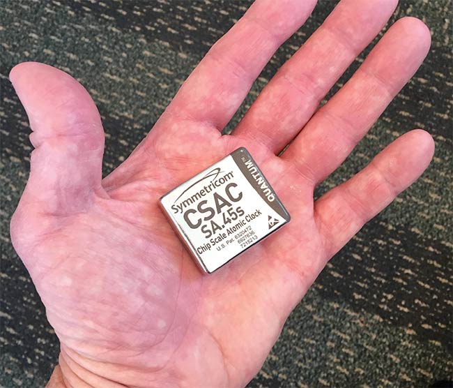
Figure 6. A commercial VCSEL atomic clock.
Feng believes the uses of future microlaser devices will spring from VCSEL technology just as VCSELs have replaced LEDs for data links and smartphone 3D imaging. In 2004, he and Holonyak created a transistor laser that operates for laser light as a standard transistor does for electricity.
Transistor lasers could, for example, greatly increase both optical data communication links and onboard computer communication. “VCSELs may reach an upward limit at 70 Gb/s, but we could go quite higher with transistor lasers,” Feng said. “There’s a lot of opportunity for us, but the difficulty on the transistor laser is that nobody is in front of us. We are the only ones [who are] going to figure out all the problems.”
Farooq Ahmed
https://www.linkedin.com/in/farooqtheahmed
Acknowledgments
The author would like to thank Axel Scherer, California Institute of Technology (Caltech); Craig Thompson, Finisar; Luke Smithwick, TriLumina; Jack Jewell, GreenVcsel; and Milton Feng, University of Illinois at Urbana, Champaign.
References
1. Sinha G. Gaurav (August 2018). Vertical-cavity surface-emitting lasers (VCSELs): Technologies and global markets,
www.bccresearch.com/market-research/photonics/vertical-cavity-surface-emitting-lasers-vcsels-technologies-and-global-markets-pho011c.html.
2. Milton Feng et al. (June 2018). Oxide-confined VCSELs for high-speed optical interconnects. IEEE Journal of Quantum Electronics, Vol. 54, No. 3, https:/doi.org/10.1109/JQE.2018.2817068.