A novel class of particle absorbers, called transferable hyperbolic metamaterial particles (THMMP), has shown selective, omnidirectional, tunable, broadband absorption when closely packed. The novel material, which absorbs more than 87 percent of near-IR light at 1200- to over 2200-nm wavelengths, with a maximum absorption of 98 percent at 1550 nm, could be used for energy, automotive and stealth applications.
The thin, flexible, light-absorbing material, a near-perfect broadband absorber, can absorb light from every angle. According to researchers, it could be customized to absorb certain wavelengths of light while letting others pass through. Materials that “perfectly” absorb light already exist, but they are bulky and can break when bent. Also, they cannot be controlled to absorb only a selected range of wavelengths.
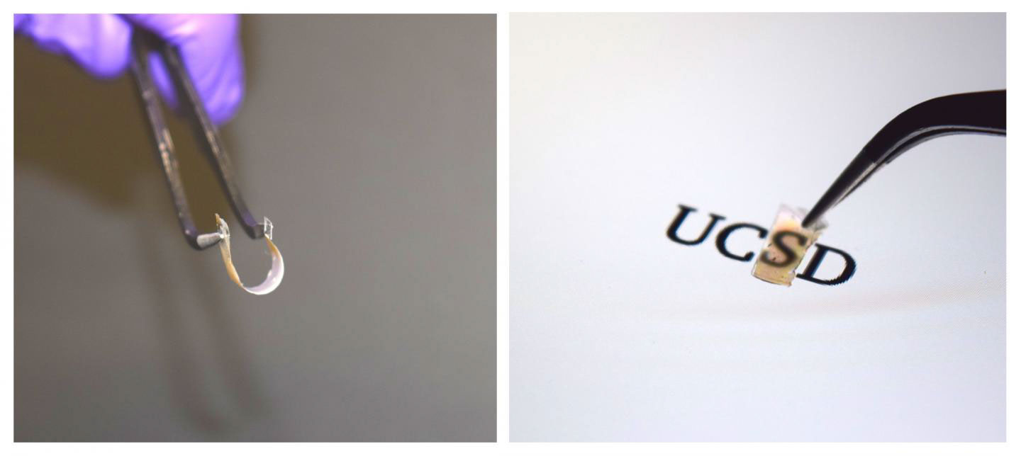
A near-perfect broadband absorber that's thin, flexible and transparent in visible light. Courtesy of UC San Diego Jacobs School of Engineering.
The tunability of the novel material relies on surface plasmon resonances, which occur on the surface of metal nanoparticles upon interaction with certain wavelengths of light. Because they can carry high amounts of free electrons, metal nanoparticles exhibit strong surface plasmon resonance in visible light but not in IR.
Researchers at the University of California, San Diego, surmised that if they could change the number of free electron carriers in the metal nanoparticles on the surface of the material, they could tune the material’s surface plasmon resonance to different wavelengths of light.
“Make this number lower, and we can push the plasmon resonance to the infrared. Make the number higher, with more electrons, and we can push the plasmon resonance to the ultraviolet region,” said professor Donald Sirbuly.
In order to control the number of free electron carriers on the metal surface, the researchers built an absorber from zinc oxide and combined it with its metallic version, aluminum-doped zinc oxide, which can hold a high enough amount of free electrons to give it plasmonic properties in the IR.
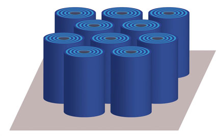
Aschematic of the nanotube array. Courtesy of UC San Diego Jacobs School of Engineering.
The materials were combined and structured using nanofabrication technologies, then deposited one atomic layer at a time on a silicon substrate to create an array of standing nanotubes, each made of alternating concentric rings of zinc oxide and aluminum-doped zinc oxide. The hyperbolic nanotube array was then transferred from the silicon substrate to a thin, elastic polymer. The material exhibited mechanical flexibility and visible transparency while maintaining near-perfect absorption at telecommunication wavelengths, even after being transferred to the polymer.
"This material offers broadband, yet selective absorption that could be tuned to distinct parts of the electromagnetic spectrum," said professor Zhaowei Liu.
“There are different parameters that we can alter in this design to tailor the material’s absorption band: the gap size between tubes, the ratio of the materials, the types of materials and the electron carrier concentration. Our simulations show that this is possible,” said researcher Conor Riley.
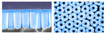
SEM images of a nanotube array: side view (left) and top view (right). Courtesy of UC San Diego Jacobs School of Engineering.
The nanoparticle-based design is potentially transferrable to any type of substrate and could be scaled up to make large surface area devices, such as broadband absorbers for large windows.
Potential applications for the near-perfect broadband absorber include transparent window coatings for buildings and cars, devices for improving solar cell efficiencies, and shields for blocking thermal detection. The researchers continue to explore different materials, geometries and designs to develop absorbers that work at different wavelengths of light for various applications.
The research was published in Proceedings of the National Academy of Sciences (doi: 10.1073/pnas.1613081114).