The atomic force microscope enables atomic- and molecular-scale visualization and measurement, functional mapping of surfaces and molecular-level manipulation.
F. Michael Serry, Veeco Instruments Inc.
Understanding the structure, function and stimulus response of individual molecules and other nanoscale structures is becoming increasingly important in research in all branches of hard sciences, in engineering and in materials development. The atomic force microscope (AFM) is a metrology tool that combines the requisite resolution with the ability to work with unmodified samples in various environments, including liquids. But AFM goes well beyond metrology to include nanometer-scale functional testing and mapping of surfaces, and even surface modification and manipulation.
AFM operation is conceptually straightforward. A hyper-fine tip on the end of a microfabricated cantilever is brought into contact or near contact with the test sample surface. (Common materials for the tip include single-crystal silicon and silicon nitride.) The tip is affected by forces interacting with the sample surface, which are initially attractive and then become repulsive as the tip contacts the surface. This contact may be perpetual (contact mode) or intermittent (TappingMode AFM). The tip-sample interactions are detected by bouncing a laser beam off the cantilever and measuring its movement with a position-sensing photodetector. Centimeters-long optical leverage and stringent vibration isolation enable routine measurement of subangstrom cantilever deflections.
The cantilever (or the sample) is mounted on a three-dimensional precision actuator — usually a piezoelectric tubelike structure. Most commonly, the actuator is used to maintain a constant interaction strength between the sample and the tip. The strength of the interaction is sometimes measured in cantilever deflection — as in contact-mode AFM — or sometimes in the amplitude and phase of the oscillating cantilever — as in TappingMode AFM. By raster-scanning the tip across the sample or the sample under the tip, a quantitative topographic map of the surface can be created based on the piezo voltage needed to maintain constant interaction strength. The in-plane (X-Y) resolution is mainly limited by the radius of the tip and often is 2 nm or sometimes even better. The resolution in the vertical (Z) dimension is not directly related to the tip and often is better than 0.5 Å.
It is possible that the tip may displace or drag delicate surface features. For delicate samples, such as biomaterials and polymers, shear forces are nearly or completely eliminated by operating the instrument in TappingMode AFM.
Probing functionality
AFM advances have enabled this technology to go far beyond making measurements of features on sample surfaces. Tip-sample interactions can be used to map electrical, mechanical, magnetic, chemical and even biological properties with nanometer-scale resolution. The latest generation of hardware and software advances, such as those in Veeco Instruments Inc.’s NanoScope V, enable the recording of events on the nanometer scale with unprecedented time resolution. These events can involve, for example, the unraveling of the tertiary structure of a synthetic or organic macromolecule or the mechanical response of a thin film to a localized force from the AFM cantilever-tip assembly, such as is present in AFM-based nanomechanical testing.
In LiftMode, the AFM can sense electrical and magnetic attraction/repulsion between the tip and the sample surface. The field distribution and field gradient above the sample can be mapped using an appropriate tip material. Alternatively, the tip can be functionalized with a chemical functional group to map different chemical species on the sample surface with molecular resolution.
A useful technique for tribological studies is lateral force microscopy, where the AFM maps friction forces between the probe tip and the sample surface. Another technique is nanoindentation mapping, which is utilized to investigate material hardness. Here the AFM measures the amount of surface deformation, as vertical force is locally applied by a tip (often made of single-crystal diamond). The same tip can be used to perform scratch-and-wear tests on the adhesion and durability of thin films.
In semiconductors, polarity and relative concentration of majority carrier (dopant) atoms can be mapped using scanning capacitance microscopy, and local variations in resistivity can be mapped with scanning spreading resistance microscopy. And in piezoelectric materials, the piezo activity can be mapped using a conductive tip.
The latest AFMs do more than measure, they enable the tip to actively modify a surface, creating nanometer-scale patterns and structures in the plane, or to induce and measure out-of-plane deformations of adsorbed species. For example, the AFM can measure the shape and distribution of DNA molecules, and then, with just a mouse click, the tip can grab a single DNA molecule off the surface while measuring the forces that bind the molecule to that surface (Figure 1).
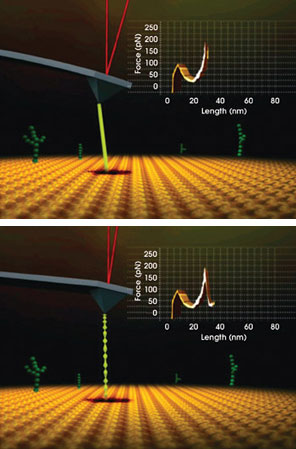
Figure 1. When used for studying polymers such as DNA, AFM can visualize the shape and distribution of molecules, measure their dimensions and, with a point and click of the computer mouse, grab a single molecule (top) while measuring the forces that bind it to the surface or the forces that bind different parts of it to each other (bottom). The same tip can image the aftermath on the surface.
Laser patterning
Perhaps the most fundamental application for AFM in nanotechnology is state-of-the-art metrology that enables development and optimization of fabrication techniques. An interesting nanolithography method of potentially widespread importance has been pioneered by a group led by Nils Hartmann at the University of Duisburg-Essen in Germany. This team has used 514-nm light from an argon-ion laser to fabricate structures and patterns that are 100 nm in size — far smaller than the diffraction limit for this wavelength.1
The key to this photothermal method is a material system whose removal process has a highly non-linear dependence on laser power. Specifically, the system comprises a molecular monolayer of alkylsiloxane deposited on a silicon wafer. Hartmann said that they use beam-focusing optics with a 0.25 numerical aperture to yield a spot diameter of 2.5 μm (1/e2). Laser irradiation results in a local temperature rise with a lateral distribution similar to the intensity variation across the laser spot (Figure 2). This, in turn, initiates a chemical reaction — removal of the alkylsiloxane monolayer.
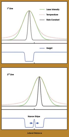
Figure 2. In this schematic drawing of the photothermal patterning strategy, the green, red and black curves depict the intensity profile of the laser spot, the temperature profile and the lateral variation of the rate constant, respectively. The blue curves show the height profile after writing the first and second lines, as displayed at top and bottom, respectively. The blue arrows at the bottom indicate the narrow (and sharp edged) stripe of the monolayer, which is left between the laser-written lines after patterning. Courtesy of Daniel Dahlhaus, Steffen Franzka, Eckart Hasselbrink and Nils Hartmann, Fachbereich Chemie, University of Duisburg-Essen,Germany.
For this monolayer, the overall process is highly activated; that is, the corresponding rate constant exhibits a strong exponential dependence on local temperature. Consequently, the initiated reaction profile is much narrower and steeper than the laser intensity profile. At fast writing speeds, the ablation threshold is reached only at the very peak of the laser profile. The result is a sharp line, with an edge width of less than 100 nm. Successive irradiation along two adjacent lines leaves a narrow stripe with a width as small as 80 nm. Small dots can be similarly created.
The process is followed by some robust wet chemistry that activates the stripe, allowing it to be used as a template to assemble electronically or photonically relevant structures. For example, gold nanoparticles from a colloidal suspension have been shown to self-assemble into long chains (Figure 3). Such nanoparticle structures could form the basis for subwavelength waveguides. They also could be converted into more compact metallic structures by standard plating techniques for use as nanowires.
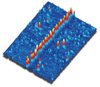
Figure 3. This AFM image shows a chain of 16-nm gold nanoparticles deposited on a postfunctionalized, laser-written alkylsiloxane stripe (scan size 1.2 × 1.6 μm). Courtesy of Daniel Dahlhaus, Steffen Franzka, Eckart Hasselbrink and Nils Hartmann.
Several aspects of this work merit further mention. First, the AFM provides the requisite spatial resolution to measure both the width of these narrow stripes as well as their depth, which is only 1.6 nm or even smaller. Just as important, the TappingMode AFM enables the gold-coated stripes to be measured without any risk of dislodging the weakly bound nanoparticles. “AFM simply is the method of choice to characterize these samples,” Hartmann said.
Piezo-response force microscopy
A technique known as piezo-response force microscopy uses the fact that, when a voltage is applied to a piezoelectric material, it expands or contracts depending on the polarization orientation as related to its internal molecular crystallographic structure. By applying an AC voltage to the sample via a conductively (Au or Pt) coated AFM tip, the local surface deformation can be measured simultaneously by the same tip. Thus, the technique can map the piezo response and, hence, the polarization orientation, on the nanometer scale.
Sergei Kalinin’s group at Oak Ridge National Laboratory in Tennessee has successfully used piezo-response force microscopy to investigate subjects as diverse as ferroelectric domain structure and growth — which are highly relevant to the development of future data storage tools — as well as structural molecular systems in biological samples such as teeth.
Ferroelectric materials offer the potential to replace magnetic-based data storage media with an increase in storage density by a factor of 10 to 100. Methods that consistently generate minimum domain sizes are needed. This task requires development of techniques that can probe the dynamic processes involved in domain nucleation and growth and the role of local microstructure on these processes. By studying local hysteresis effects in a technique called switching spectroscopy piezo-response force microscopy, the researchers can see the effects of material defects on the switching of domains.
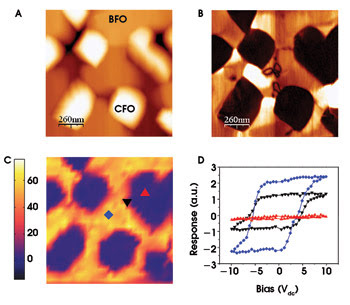
Figure 4. These images show the topography of multiferroic BiFeO3-CoFe2O4 (BFO-CFO) nanostructures (A) and the corresponding piezo-response force microscopy amplitude image (B). The ferroelectric and antiferromagnetic BFO show piezo response, while the ferromagnetic CFO spinel pillars show no piezo response. The image in C shows the 2-D SS-piezo-response force microscopy map of the work of switching (area of hysteresis loop), and D shows the representative loops from BFO, CFO and the BFO-CFO heterostructure interface. The piezo response near the interface is roughly half that of the BFO itself, suggesting a reduction caused by clamping effects. Image courtesy of B.J. Rodriguez, S. Jesse and S.V. Kalinin, Oak Ridge National Laboratory. Sample courtesy of R. Ramesh, University of California, Berkeley.
“In many instances, researchers regard imaging in liquid as a limitation narrowing the applicability of electrical scanning probe microscopy,” Kalinin said. But in the case of piezo-response force microscopy, they have shown that, in an aqueous environment, long-range electrostatic forces are eliminated, resulting in a significant enhancement in spatial resolution. “This potentially allows our research to be extended to biological materials which often demonstrate piezoelectric activity because they contain oriented polarized molecules and often possess complex electromechnical responses.”
The team recently published AFM data on the orientation of collagen within fibrils in teeth. Obtaining this data required a spatial resolution of 10 nm.
Bacterial spores
Another group studying in vitro biomaterials — bacterial spores — is led by Alexander J. Malkin at Lawrence Livermore National Laboratory in California. When starved for nutrients, Bacillus cells initiate a process of sporulation that results in the formation of metabolically dormant spores. Spores can remain dormant for extended periods, and they exhibit a remarkable resistance to adverse environmental insults, including heat, radiation and toxic chemicals that are lethal to vegetative cells. The resistance of dormant spores is attributed to multilayer spore architecture.
Using the AFM, Malkin and Marco Plomp have visualized the high-resolution native spore coat architecture of various Bacillus species (Figure 5). They found that strikingly different species-dependent spore coat structures are a consequence of nucleation and crystallization mechanisms that regulate the assembly of the outer spore coat.2,3
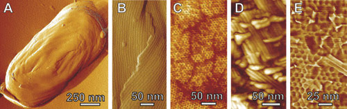
Figure 5. Atomic force microscopy provides high-resolution images of native spore coat structures. The outer spore coats of (A,B) Bacillus atrophaeus consist of crystalline layers of single-domain rod-shaped structures, while the outer coat of (C) Bacillus thuringiensis consists of a honeycomb structure. Bacillus cereus spores’ (D) outer coat is formed by a multidomain rodlet structure and has (E) a honeycomb structure beneath. Data courtesy of Marco Plomp and Alexander J. Malkin, Lawrence Livermore National Laboratory, Livermore, Calif.
Malkin noted that the unique ability of the AFM to obtain nanometer resolution in vitro is key to their work. “Identification and characterization of protein surface structures of bacterial spores is critical to elucidating mechanisms of pathogenesis and immune response and could lead to the development of vaccines, detection systems and improved decontamination efforts.”
Malkin and Plomp also have developed experimental approaches to directly probe structural dynamics of individual bacterial spores in response to environmental changes. These studies establish that the dormant spore is a dynamic physical structure that provides an experimental platform for investigating spore structural dynamics, germination and response to decontamination regimes.
AFM technology has come a long way since its inception in 1986. Today’s advanced AFMs not only make it possible to visualize and measure — in three dimensions — nanometer-scale and even atomic-scale features — in air, in liquids and in vacuum — but they also allow material property examination and manipulation on that same level in all those environments, which is truly unique in science and technology instrumentation.
Meet the author
F. Michael Serry is senior applications scientist at Veeco Instruments Inc. in Santa Barbara, Calif.; e-mail: [email protected].
References
1. D. Dahlhaus et al (2006). 1D nanofabrication with a micrometer-sized laser spot. NANO LETT, Vol. 6, pp. 2358-2361.
2. M. Plomp et al (2005). The high-resolution architecture and structural dynamics of Bacillus spores. BIOPHYSICAL JOURNAL, Vol. 88, pp. 603-608.
3. M. Plomp et al (2005). Bacillus atrophaeus outer spore coat assembly and ultrastructure. LANGMUIR, Vol. 21, pp. 10710-10716.