NANJING, China, Nov. 18, 2020 — Researchers from Nanjing University are using metalenses to enhance and shrink microscopes while maintaining resolution with a large field of view.
In pursuit of a more compact integrated microscope system, Tao Li, professor of engineering and applied science, and his team mounted a metalens on a CMOS image sensor to create a prototype of an imaging system that is roughly the size of a coin. The metalens-integrated imaging device (MIID) features an ultracompact architecture with a working imaging distance in the hundreds of micrometers. A simple image stitching process enabled the researchers to obtain wide-field microscope imaging while preserving a large field of view and high resolution.
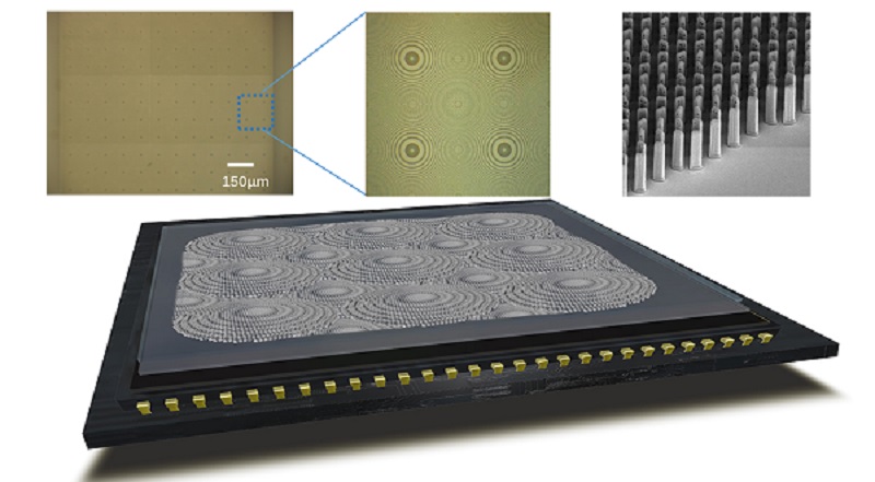
Metalens-integrated imaging device. Courtesy of Nanjing University.
The imaging system has a millimeter-size silicon metalens consisting of a 6 × 6 array. Even though there are multiple lenses integrated into the system, the imaging distance remains small, approximately 500 μm, due to the small size of each lens — approximately 200 μm.
According to the researchers, the lens can be expanded to the centimeter scale to cover the full CMOS sensor.
The array — a polarization multiplexer — has two distinct phase profiles that correspond to two circular light polarizations. According to Li, the arrangement ensures the elimination of blind spots.
The researchers note that the performance of the device will need improvement, and they have proposed approaches such as adopting low-loss materials including GaN and SiN. The researchers hope that the prototype will usher in an era of pocket microscope systems.
The research was published in Advanced Photonics (www.doi.org/10.1117/1.AP.2.6.066004).