As high-volume manufacturing helps metalenses make their debut in consumer electronics this year, the prospects for the technology’s growth are anything but flat.
JAMES SCHLETT, CONTRIBUTING EDITOR
Earlier this year, the first wave of smartphones equipped with STMicroelectronics’ second-generation direct time-of-flight (TOF) sensor reached the consumer market. The sensor includes planar metasurface optics.
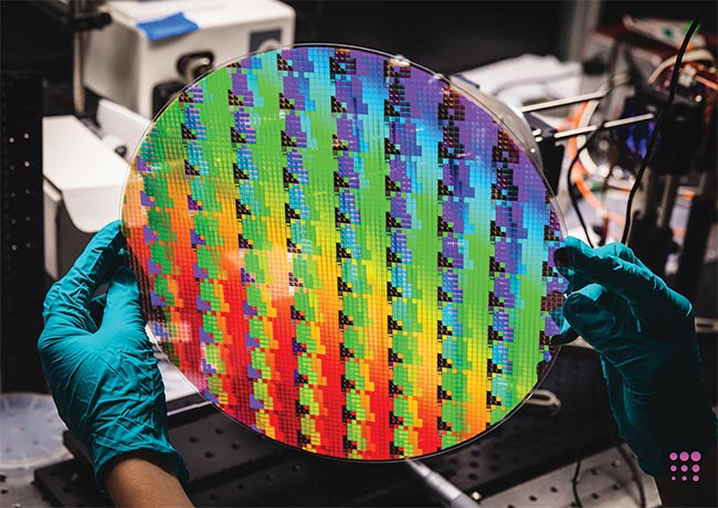
The high-volume lithography processes on which semiconductor manufacturing has relied for decades can be adapted to fabricate the nanosurface structures of metaoptics. A 12-in. Metalenz wafer, for example, encompasses about 5000 metaoptics. Courtesy of Metalenz.
The metalens-enabled sensor will assist the main camera’s autofocus function by providing accurate distance measurements in multiple zones at speeds between 30 and 60 fps. Speedier focus enhances imaging in low-light and other settings by providing reliable distance-to-object reference data, according to Andy Price, STMicroelectronics’ imaging module R&D director.
The rollout of the smartphones, made possible through a partnership between STMicroelectronics and the Boston-based startup Metalenz, represents the introduction of the world’s first consumer electronics device with this type of optical metasurface technology. The metalenses for STMicroelectronics’ new direct TOF sensor are composed of a binary structure of nanopillars etched onto thin glass wafers. The nanopillars enable control of light in ways that would be unachievable with conventional refractive lenses.
“The success of metasurface optics relies on engineering of the scattering properties of the surface nanostructures, resulting in unprecedented control over electromagnetic radiation with a single layer of material,” Metalenz’s co-founder and CEO, Robert Devlin, said.
The first generation of these metasurfaces to be commercialized by companies such as Metalenz and NIL Technology worked in the NIR, where the technology was well-suited for indirect and direct TOF devices. STMicroelectronics believes this technology could spread across an even wider product portfolio, according to Price.
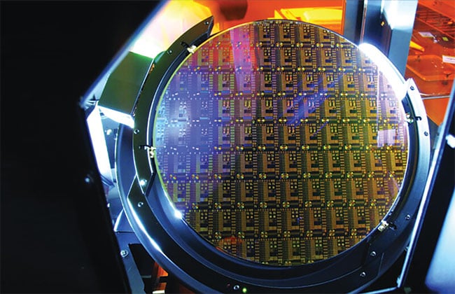
Smartphones that incorporate metalens-enabled direct time-of-flight cameras will reach stores early this year, debuting the first consumer electronics products to feature metasurface technology. Courtesy of STMicroelectronics.

NIL Technology is developing meta-optical elements aimed at significantly reducing the size and complexity of smartphone camera lens systems. Courtesy of NIL Technology.
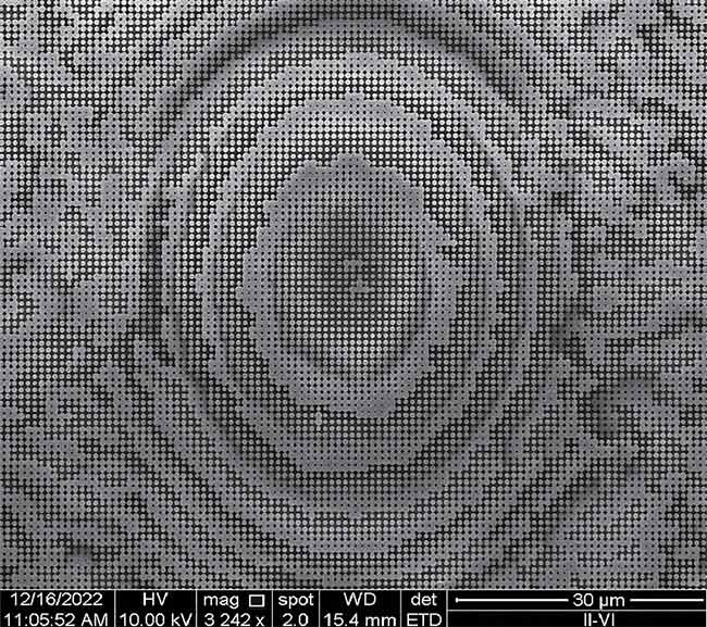
A top-down scanning electron microscope image shows a focusing splitter with aberration correction based on a metaoptical element that combines multiple functions into a single optical surface. Courtesy of Coherent.
“This is game-changing. For the first time, you’re going to have the same foundry making the same system. Now, it’s separate: If you take a camera module for a cellphone, there are four plastic lenses that have to be aligned very carefully, and there is a CMOS sensor made by different technology,” said Federico Capasso, Metalenz’s other co-founder and a Harvard University physics professor.
Meta something
Prior to the rollout of its direct TOF sensor with Metalenz’s metasurface technology, STMicroelectronics was already manufacturing diffractive optical elements (DOEs) on 300-mm wafers. “Moving to a metasurface lens enabled much more functionality on the same surface at almost no additional cost,” Price said.
Rajesh Menon, an electrical and computer engineering professor at the University of Utah, cautioned against overly liberal use of the term “metalens,” which actually describes a subset of diffractive lenses. Also, the overlap in the terminology that companies use to describe their metalenses belies a range of different manufacturing processes and architectures. Where Metalenz refers to “meta-optics,” for example, NIL Technology offers “meta optical elements” (MOEs), and Coherent supplies “metaoptics.”
“I do not believe there is a strict, commonly accepted definition of metaoptics and diffractive optics.” said Dmitri Iazikov, Coherent’s director of product management. “We now try to use metaoptics rather than diffractive optics, as it’s considered a more exciting term.”
Coherent’s metaoptics provide beam-shaping and beamsplitting functions at 940 nm. Phase transformation occurs within an approximately 1-µm-thick layer of the metamaterial. Coherent envisions that its beam-shaping optics metalayer will ultimately be monolithically integrated with active light-generating chips, such as VCSELs and micro-LEDs, creating an “ultimate light generator on a chip,” according to Iazikov.
In 2021, Copenhagen, Denmark-based NIL Technology launched a mass production-ready 940-nm imaging lens with a single metasurface illuminated by a VCSEL. NIL Technology manufactures both DOEs and MOEs, which share many of the same properties. “One differentiator is that MOE can treat different polarizations of the light differently,” company CEO Theodor Nielsen said.
NIL Technology’s DOEs are composed of a multilevel structured surface that creates a phase delay of light impinging on it. This phase delay is what causes the diffractive interaction, Nielsen said. His company fabricates its DOEs by replicating surface structures into a polymer on a glass substrate. These structures are then hard-cured with UV light. The length scale of the structures in the xy dimension corresponds to some targeted scale of the light, such as from 1:4 to 1:1 of the wavelength.
Where many conventional diffractive lenses are based on a quasi-periodic structure, such structures on a metalens are generally smaller than the wavelengths they influence. Metalenz further draws a distinction between the two by noting that when light passes through a metalens’s nanostructures, it induces a phase shift with a controllable flow, which is similar to beam forming. In contrast, when light passes through the coarser, grooved structures of Fresnel lenses, it bends according to refractive and diffractive principles, yielding less pattern control.
The question
STMicroelectronics’ shift from diffractive lenses to metasurfaces was in many ways triggered more than decade earlier by a single question. The question was posed to Capasso in 2008 by his colleague James Anderson, an expert in atmospheric chemistry who pioneered research on the ozone hole. Anderson wanted to fly a drone equipped with a quantum cascade laser around the North Pole. Because the drone had little room to spare, Anderson asked Capasso if he could make the laser smaller by eliminating the lens mounted in front.
“That was a good question,” said Capasso, who published his solution in the journal Science in 2011. The paper described how to design metastructures, and it formed the foundation for the meta-
surface field. Capasso followed it with a second paper, published in Science in 2016, that demonstrated the application of metalenses to visible wavelengths, along with diffraction-limited focusing and subwavelength-resolution imaging techniques. That same year Capasso
co-founded Metalenz with Devlin, one of his graduate students at the time. Two years later, the startup was manufacturing high volumes of demonstration wafers.
Much has changed since then, most notably the manufacturing processes through which metalenses are made.
Lithography, the high-volume process on which the semiconductor manufacturing industry has relied for decades, can be adapted to fabricate the nanosurface structures of metalenses, Capasso said.
Metalenz’s technology, manufactured in standard semiconductor foundries, requires a single step of lithography. As the company scaled up manufacturing, it encountered challenges with producing designs that could be fabricated within the constraints of the tolerances that were achievable by its foundry partners. Devlin said he does not see any more manufacturing hurdles for the first generation of metalenses, but future generations could bring more challenges. “As we look to the future of our designs, some of the nanostructures are more complex shapes or may require more exotic materials,”
he said.
The first generation of NIR metalenses leverages silicon-on-glass substrates. A group led by Capasso demonstrated the potential for mass-producing large, 1-cm-diameter metalenses on 4-in. fused-silica wafers. Each metalens had approximately 160 million nanopillars etched into it via deep ultraviolet lithography.
“Silicon has the best material properties for these wavelengths and has the added advantage that it is the preferred material from our foundry partners,” Devlin said. “Generally, what makes a good material for a metasurface is one that has a high refractive index and low absorption at the wavelength of interest.”
Another highly refractive material with potential for metalenses operating in the visible range is titanium dioxide (TiO2), but the University of Utah’s Menon considers the material to have a disadvantage. “One can achieve basically the same performance with polymer-based diffractive lenses,” he said. “For IR applications, other materials are interesting, such as sapphire, germanium, [and] ZnSe.”
NIL Technology uses the lithographic nanoimprint technique to make nanostructures, and the company usually uses e-beam lithography for prototyping. According to Nielsen, the method enables MOEs made from amorphous silicon to be effectively a patterned film on top of glass. Each of these structures is referred to as a meta-atom and acts as a resonator that determines how light is transmitted from it. “The propagation of light from all the meta-atoms gives the diffractive pattern that determined the optical performance,” Nielsen said.
Although Nielsen described nanoimprint techniques as “the lithography of choice” to make the meta-atoms, Capasso said nanoimprint lithography cannot yet access the high volumes that are possible
through other lithography methods — partly because it is very difficult to displace such a highly developed, scalable,
and successful technology. “Metalenz is riding the wave of established foundry-based semiconductor technology to launch CMOS-compatible flat optics,” Capasso said.
At STMicroelectronics, however, Price foresees challenges in mass-manufacturing metalenses for camera sensors in the broadband visible range. This will still require conventional refractive optics. “Due to the complexity and ultrasmall-scale nature of the structures required
for broadband optical metasurfaces in
visible wavelengths, a significant barrier
to entry remains even for advanced photolithography fabrication techniques,” he said. “Metalenses have different advantages and capabilities compared with standard refractive lenses, and it is logical to have a blend of metasurface and diffractive optical elements.”
Future applications
Echoing Price, Capasso said, “We’re
not talking of the demise of refractive optics. That would be complete nonsense. Refractive optics are here to stay. But there are so many applications for high volume [metalenses].”
Cellphone-makers are not the only end market for metalens-enabled TOF cameras. AR/VR, health and wellness, and retail all offer further market opportunities.
“Metaoptics improve TOF signal-to-noise ratio, which can allow the system to maintain the same resolution with lower transmit power, which results in longer battery life,” Devlin said.
Optical sensors for the automotive industry are presenting further opportunities for metalenses, especially for lidar, advanced driver assistance systems, and driver monitoring cameras.
“We see large interest in the automotive industry to develop new solutions, and this drives a lot of our engagements,” Nielsen said.
Devlin agreed. He said Metalenz’s ability to create complex and precisely controlled patterns with high contrast and high uniformity in a single metaoptic offers the unique ability to capture polarized light information. In practical terms, this allows automotive imaging systems to peer through glare and fog and detect the presence of black ice on the road, for example.
Another emerging application is facial recognition, especially for Metalenz’s polarization-sensitive metasurface optics solution for 3D sensing. This optical
module can map polarization information
in an imager’s entire scene without the use of filtering or the loss of signal strength. This provides information about 3D material surface characteristics,
increased shape contrast, and the molecular makeup of surfaces — all with a
single metasurface optic and sensor. The module could also potentially shrink a full-Stokes polarization sensor by about 5000×, according to Devlin.
The polarization sensitivity enabled by metalenses promises to make smartphone face recognition 100% reliable and more able to differentiate between an actual face and the picture of one, Capasso said. “Polarization gives depth. That’s a higher level of security.”
Structured darkness
Metalenses can structure darkness as well as light by creating optical phase singularities, where dark is surrounded by light. Last year, a group led by Capasso detailed how these singularities are formed1. The team wrote, “Optical singularities are formed at the intersection
of the zero-isosurfaces of the real and imaginary parts of a complex field (e.g.,
a linearly polarized electric field).”
“The beauty of that is [that] dark does not have any fractural limit,” Capasso said. “I can make the dark spot as small as possible, much smaller than the wavelengths. I don’t know what the applications can be, but I have some ideas. If I have structured dark, I can use it to probe materials, for example, at very fine scale if there are defects and so forth.”
Reference
1. S.W.D. Lim et al. (2021). Engineering phase and polarization singularity sheets. Nat Commun, Vol. 12, No. 4190, www.doi.org/10.1038/s41467-021-24493-y.