MARIE FREEBODY, CONTRIBUTING EDITOR
Prepare for optical metamaterials to enter our pockets, kitchens, cars, and offices in the next three to five years. That’s what experts in the field predict. Thanks to rapid maturation of technology and falling production costs, the doors are opening to some lucrative new markets for the materials.
Optical metamaterials leverage either chemical compositions or surface features that are smaller than certain wavelengths of light to enable them to interact with photons in useful ways. From damage-resistant antireflective optics to tunable flat lenses, metamaterials have already made commercial inroads. Now they are finding employment in smartphones, cameras, cars, and gaming consoles. And the most immediate consumer application appears to be depth-sensing in mobile devices, driverless cars, and augmented and virtual reality headsets.

From damage-resistant antireflective optics to tunable flat lenses, metamaterials promise more versatile and compact optical systems for smartphones, cameras, automotive safety systems, and gaming consoles — and sleeker augmented reality headsets. Courtesy of Corning.
Metamaterials science operates at the intersection of materials informatics, engineering, materials science, and physics. Although metamaterials targeting microwave frequencies have been successfully harnessed for wireless technology for over a decade, the optical arena proves more problematic, but potentially more lucrative to those who can address early challenges with the technology.
One challenge to transforming an optical material into a metamaterial involves intricately patterning its surface with nanostructures, which then locally manipulate the propagation of light. Nanoscale patterning on a large scale is only now looking possible.
Optical metamaterials have until now been largely held back by lack of production infrastructure and a shortage of device designers familiar with the technology. But a growing number of startups and large corporations are showing interest in the use of digital patterning for faster product design.

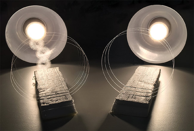
Metamaterials enable flat optical components to impart both diffractive- and refractive-type functions in a single layer. This dual functionality can cut the number of components in a dot pattern projector — a complex module that structures light for facial recognition in mobile phones — thereby enabling the projectors to be made more compact. Courtesy of Metalenz.
Metamaterials already manipulate light with greater control than conventional
optics. This control manifests as “shortcuts” that allow optical elements to achieve equivalent or better performance. Metamaterials also introduce functionalities that are unachievable with conventional optics. They can, for instance, help challenge diffraction limits, capture
evanescent waves, break reciprocity, or combine multiple functions — such as heating and optical filtering — within a single, ultrathin material stack. By harnessing existing production techniques, metamaterials have set the stage to further expand optical design freedoms and enable fabrication of thinner, lighter, lower-cost, and more sustainable optical components that are ripe for commercialization.
According to a report by Lux Research, initial commercial deployment of optical metamaterials is projected to reach $50 billion by 20301. Sensational future prospects for the technology, such as invisibility cloaks, initially caught the attention of mainstream media. But in reality, the first products based on optical metamaterials have already entered the lens market. In the next three to five years, the most valuable sectors are predicted to be cellphone cameras and corrective lenses, along with the expectation of improvements to lasers, solar cells, lidar systems, and driverless cars.
Bottlenecks remain, however. Currently, only a handful of developers are leading this technology, and as top engineering graduates in the field are snapped up by the aerospace and defense industry, there is limited awareness of the technology’s potential beyond those sectors.
Additionally, although metamaterial production costs are falling rapidly, the price tag for many fabrication techniques remains prohibitively high, and they have struggled to scale up sufficiently for high-volume industries such as automotive, consumer electronics, and energy. In a bid to overcome these challenges, innovative
photonics specialists are teaming up with larger corporations to harness their manufacturing expertise as well as their foundries. As a result, commercialization could soon become a reality.
The road to commercialization
Aleksandra Boskovic, director of Optics, Surfaces, and Integration Technologies at Corning Research & Development Corp., likens the development of optical metamaterials to the silicon revolution, which transformed electrical components into efficient, miniaturized circuits in the 1970s. Boskovic said that metamaterials will similarly make optical components more compact and multifunctional.
Startups will likely play a vital role in this process if the silicon revolution is an accurate model. The integrated circuit (IC) industry divided chip development between fabless companies that specialized in designing ICs and the foundries that manufactured them. The same industry model could be applied to photonic metamaterials.

Metamaterials offer the versatility to improve
light collection in 3D sensing systems while reducing the overall number of optical
components. These features are attracting the consumer electronics industry’s interest. For
example, smartphones can leverage the technology to incorporate more compact facial recognition systems. Courtesy of Corning.
Edgehog Advanced Technologies has managed to eliminate reflection from optical glass surfaces at all viewing angles,
without the use of coatings. The technology it developed, illustrated by these glass substrates, leverages metamaterials and has potential benefits for wide-angle cameras and displays, as well as solar panels. Courtesy of Edgehog.
Boskovic believes that metamaterials will be a game changer in the field of
optics. Both startups and large companies, including Corning, will play a key role in this transformation through innovation in new metasurface designs, materials, and processes.
The surfaces of metamaterials — that is, metasurfaces — feature high-precision topographies that typically require specialized fabrication processes and equipment, such as those used to manufacture ICs. With no dedicated glass fabs in existence today, metamaterial designers are forced to turn to semiconductor fabs designed to work with silicon substrates.
To harness the capabilities of an IC fab, metamaterial developers must ensure that their optical material behaves like a silicon wafer. Corning is currently devising specialty glass materials and wafers that it hopes will work seamlessly in a typical silicon fab. This will enable the fab to make metasurface products on glass when needed, said Xavier Lafosse, commercial technology director of Advanced Optics at Corning Inc.
“Glass has very different optical, electrical, chemical, and mechanical properties from silicon,” he said. “Therefore, the key challenge is to make glass behave similarly to silicon using existing process and equipment infrastructure. Corning has been working in this area for the last few years with established fabs and foundries, and we have made significant progress. We are currently engaging customers and will be prepared to ramp up to production volume when the metamaterial community requires such glass wafers.”
The marriage of silicon foundries with metamaterial production could be a stroke of genius — if it can be perfected.
Harnessing established top-down fabrication techniques, such as nanoimprinting or nanomasking, will give makers the flexibility to pattern a substrate with engineered nanostructures on a variety of optical materials with almost any geometrical shape. Importantly, these metamaterials could be produced in highly scalable volumes.
Metasurfaces: first to market
Harvard spinout Metalenz, one of the early developers of optical metamaterials, believes it has cracked through these barriers to commercialization. The company recently raised $10 million from semiconductor makers — including Intel Capital, 3M, TDK Ventures, and Applied Ventures — to help make key hires and to scale production of its new lens, which is set to hit the market in 2022. With sights set on the consumer electronics and smartphone markets, Metalenz based the lens on a single, flat, metaoptical component that imparts both diffractive- and refractive-type functions in a single layer. This dual functionality can cut the number of components in a dot pattern projector, which is a complex module that structures light for facial recognition in mobile phones. Having fewer components translates as a smaller footprint. Additionally, for imaging in a 3D sensing system, the lens improves light collection while replacing up to four optical components with one metamaterial component.
“Compared to 3D metamaterials, the metasurface technology
that we produce at Metalenz does not rely on complex 3D patterning or propagation of light through a lossy material,” said Robert Devlin, co-founder and CEO of the company. “By locally engineering only the in-plane dimensions of subwavelength structures, we can produce multifunctional optical elements that significantly reduce the complexity of optical modules.”
Metalenz and its partners are currently ramping up the technology to mass production with the aim of putting the company’s first products on the market. This has largely been enabled using standard photolithography and CMOS fabrication processes.
“With our foundry partners, this allows us to produce millions of metasurface optics in a single day,” Devlin said. “The scientific precision and customization we offer will help shape the future for health care, computer vision, self-driving cars, and deskless work.”
With regard to consumer electronics applications, Devlin hopes his company’s technology will find use in 3D sensing modules for phones and laptops. “What our technology will provide compared to existing tech is a smaller, simpler 3D sensing camera that will allow you to
see farther and save battery life,” he
said.
Antireflective coatings are often
applied to optical systems to optimize their performance in applications such as solar panels, displays, lenses, and sensing systems. In automotive cameras, for example, glare and flare can interfere with image recognition when the sun is at low angles.
Founded in 2018, Montreal-based Edgehog Advanced Technologies has managed to eliminate reflection from
optical glass surfaces at all viewing angles, without the use of coatings. Instead, it developed a glass substrate with a nanotextured antireflective surface. The technology has potential benefits for wide-angle cameras and displays, as well as solar panels.
The company made manufacturing scalability a priority from a very early stage, said Nasim Sahraei, Edgehog’s founder and vice president of product development. “We employed, tried, and tested manufacturing equipment used in the semiconductor and flat panel display manufacturing industry for making early proof of concepts,” she said. The company hopes to scale up its production within the year.
“Manufacturing of our product has two critical steps, both of which are scaled in terms of the dimension of the glass and volume of production in the flat panel manufacturing industry,” Sahraei said. “With the help of our advisers from the industry, we have modeled the manufacturing cost for large volumes and have shown that our product cost is very competitive with existing alternatives.”

Optical metamaterials apply to more than
optical elements. The technology’s high-volume scalability and its ability to control light in unique ways on very thin substrates offer new options for enhancing the security and authenticity of banknotes. Courtesy of Meta Materials.
Since metamaterials can encode greater functionality in smaller, lighter, and lower-cost components, the lowest hanging fruit is likely to be in technology areas where performance, weight, and size are most important. George Palikaras, the president, CEO, and founder of Meta Materials Inc., expects to see more metamaterial components replacing conventional optics, especially in areas where bulky, complex optical systems are required.
“It is clear now that the key applications will utilize metamaterials in a film or [in] surface form factors as opposed to bulk metamaterials, performing functions such as complex optical manipulation, as in AR and VR systems, biosensing, thermal management in space systems, and authentication,” he said.
But metasurfaces can also be useful products in their own right. Meta Materials recently acquired Nanotech Security Corp., allowing the potential for it to introduce high-volume nanoimprint lithographic manufacturing to enhance banknote security. The company is now capable of printing plasmonic metastructures with security details smaller than
10 nm onto substrates at a rate of about 50 to 150 m per minute.
Future constraints
Given that metamaterials are already enabling companies to test new optical concepts at speeds and prices that were unimaginable a decade ago, the next three to five years are certainly going to be interesting.
Early adoption of metamaterials will depend on how easily designs and applications can be manufactured at scale,
allowing them to be provided in volume and at lower cost. But there are other limiting factors that need to be overcome.
One such constraint is the lack of integration between academics and end users. So far, much of the hype around metamaterials has focused on the features or on new physics of a metamaterial rather than on clearly communicating how these features benefit the end user.
This applies in some industries more than others. The aerospace and defense industry, for example, has a clearer
understanding of optical metamaterials
and their potential applications. As a result, the industry, as mentioned earlier, has been hiring most of the top engineering graduates in the field for the past two decades. “Many products exist, but no one beyond this industry really knows about them since most innovations are still under strict, classified, defense-funded programs,” Palikaras said.
As metamaterials gain more mainstream recognition, academic and industry professionals agree that these unusual optical materials will increasingly become an enabling technology, helping to enhance and fortify a large range of existing products simply by making them perform better and more sustainably.
Reference
1. Lux Research. Innovation digest: the Lux take on the future of optical metamaterials,
www.luxresearchinc.com/the-lux-take-on-the-future-of-optical-metamaterials-press-release-executive-summary.