A University of Delaware (UD) research team has designed an integrated photonics platform using metasurfaces. To limit the loss of data, the team fabricated a high-contrast transmitarray (HCTA)-based metalens on a silicon-based chip programmed with hundreds of tiny air slots to enable on-chip parallel optical signal processing.
The 1D metalens has a numerical aperture up to 2.14, which can focus light to within 10 µm with less than 1 dB loss. Computational tasks based on Fourier transformation (FT) can be performed by cascading multiple layers of the HCTA-based metalenses. To demonstrate FT and spatial differentiation, the researchers layered three metasurfaces together.
The platform is foundry fabrication-compatible, ultracompact, and designed to achieve on-chip wavefront transformation with low insertion loss and broadband operation.
“This is the first paper to use low-loss metasurfaces on the integrated photonics platform,” professor Tingyi Gu said. “Our structure is broadband and low loss, which is critical for energy-efficient optical communications.”
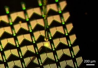
A UD research team fabricated a metalens on a silicon-based chip programmed with hundreds of tiny air slots, enabling on-chip parallel optical signal processing. Courtesy of Tingyi Gu and Zi Wang.
The UD researchers said their device is smaller and lighter than conventional devices of its type. It doesn’t require the manual alignment of lenses, so it is more scalable compared to the traditional free-space optics platforms.
The team’s experimental demonstration of the functional HCTA-based metalens could open new directions for on-chip diffractive optical systems. The on-chip metasurface could be integrated with multimode waveguides to perform mode transformation in mode division multiplexing systems.
The 1D metasurface design could facilitate novel on-chip systems with low power consumption and ultracompact dimensions, including on-chip spectrometers, light detection and ranging devices, and diffractive optical computational circuits.
“It’s just much faster than conventional structures,” said Gu. “There are still a lot of technical challenges when you try to actively control them, but this is a new platform we are starting with and working on.”
Parts of the device were fabricated in the UD Nanofabrication Facility (UDNF) and at AIM Photonics in Rochester, N.Y.
The research was published in Nature Communications (www.doi.org/10.1038/s41467-019-11578-y).