Micro-LEDs offer efficiency, brightness, and faster response times, but manufacturers must first overcome significant hurdles.
HANK HOGAN, CONTRIBUTING EDITOR
Small, as in microscopic, LEDs promise brighter displays and longer-running mobile devices, but only after manufacturers overcome several challenges. Known as micro-LEDs, these semiconductor chips are generally 10× smaller in width and length than traditional, standard LEDs. They also have different principal markets.
“The main application targets are direct-emission displays for smartphones, TVs, wearables like AR displays, smart-watches, and so on,” said Eric Virey, senior analyst for LEDs and displays at the technology market research firm Yole Développement.
For the smallest displays, those on mobile devices, micro-LEDs could lead to much longer runtime on a single battery charge. Today’s LCD and OLED displays are only about 5 percent efficient. In contrast, demonstrations of direct-emission micro-LED displays are reportedly 20 percent efficient. Since the display causes a large drain on the battery, a more efficient display would mean a mobile device could run longer, perhaps even days, on a single charge.
For larger displays, micro-LEDs potentially offer greater brightness, faster response times, and longer operating lifetime than current technology offers. Sony has created a commercially avail-able version of such a display, according to Virey. He said it costs hundreds of thousands of dollars, however, and is intended for high-end retail or corporate applications. But there are rumors of the imminent launch of more consumer-oriented, albeit also high-end, products.
Besides expense, manufacturers face other challenges in making micro-LED digital displays. “They require highly specific chip designs, manufacturing infrastructures, and assembly processes,” Virey said.

The LED landscape as of 2018. Micro-LEDs are much smaller than traditional LEDs, as this scale figure shows. Micro-LED packaging and applications differ from those of traditional LEDs.
A need for special handling, above that required for traditional LEDs, shows up in several areas. One is in chip manufacturing. Conventional LEDs, with widths or lengths below 10 μm, have leakage currents and sidewall effects that make them inefficient. The sidewall accounts for a larger percentage of the overall device, making it have a larger impact because the chip is smaller. One way this problem has been solved is via changes to chip fabrication, with many research teams reporting efficiency values in excess of 20 percent, said Virey.
Another driver for innovations in manufacturing is the formidable task of mass-producing displays. Every display may require fabricating millions of red, green, and blue micro-LEDs — the three primary colors. People are good at detecting slight visual differences across a display, so each color must emit in a narrow band to achieve the required visual quality.
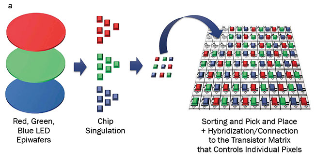
Micro-LED displays use individual red, green, and blue chips as emitters (a). An alternative approach (b) down-converts blue emitters to red and green using a conversion layer.
4K displays, for example, have the highest resolution with about 8 million pixels. Because each pixel requires one red, one green, and one blue emitter, about 25 million micro-LEDs must be manufactured for one display.
Once made, the multitude of micro-LEDs must then be transferred to a display backplane, which contains the circuitry that turns individual pixels on and off.
Adding to the challenge is consumer expectation of no dead spots. If a display shows dead pixels, either the defective micro-LEDs must be tested and repaired, or redundant chips must be placed at every pixel location, ready to act as replacements.
Finding solutions
Manufacturers are reporting progress on these hurdles. ALLOS Semiconductors GmbH of Dresden, Germany, for instance, has created a manufacturing process that meets cost and yield requirements, according to Alexander Loesing, chief marketing officer. The company licenses its technology to customers and establishes its process at customer locations.
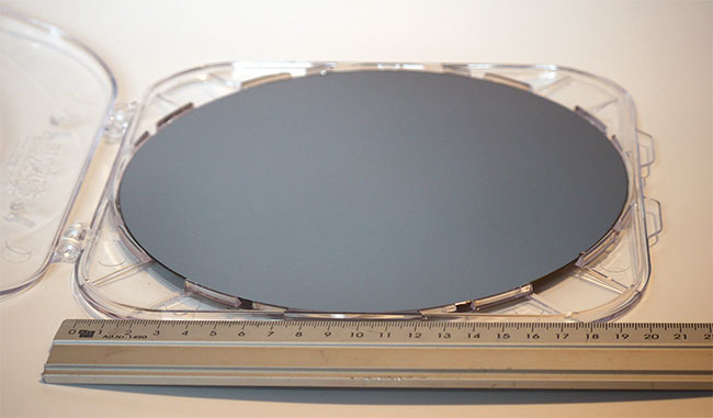
A 200-mm GaN-on-Si (gallium nitride on silicon) epiwafer that can be used in making micro-LEDs.
A primary reason the approach pioneered by ALLOS succeeds is its proprietary patented process for growing gallium nitride (GaN) on a silicon (Si) substrate, said Loesing. The manufacturing takes place in a semiconductor-grade cleanroom. In this setting, the failure rate of fabricated chips approaches the parts-per-billion required for commercially viable large-scale micro-LED manufacturing — without testing and repair.
The company says it has solved the problem of the crystal lattice mismatch between GaN and Si. The crystalline structure of the two materials must be well-matched to prevent defects and degraded LED performance. This is one reason that the traditional substrate for LED manufacturing has been sapphire, which offers a much better lattice match thanks to buffer technology.
With sapphire, however, volume-production substrates measure only 100 mm in diameter, while Si wafers measure 200 or 300 mm across. A larger substrate allows for more chips on each wafer, which leads to lower cost per chip. For ALLOS, this cost structure means its micro-LED process is ready for mass production.
The company also appears to have found a solution for achieving uniformity in pixel emissions. The human eye can pick up differences of a few nanometers in pixel emissions on a screen. To avoid detection of any variations, the peak output of each red, green, and blue micro-LED must fall within a few nanometers wavelength of each other. An extremely uniform GaN epitaxial layer is necessary to achieve consistent output.
ALLOS demonstrated this capability with the help of equipment and expertise from Veeco Instruments, which is based in Plainview, N.Y. Peak emission wave-lengths across a wafer showed a standard deviation as low as 0.85 nm, close to the industry’s ultimate emission uniformity requirements of ±1 nm. Ajit Paranjpe, chief technology officer for Veeco, said it should be possible — through careful selection and matching of different regions on a wafer — to hit the target.
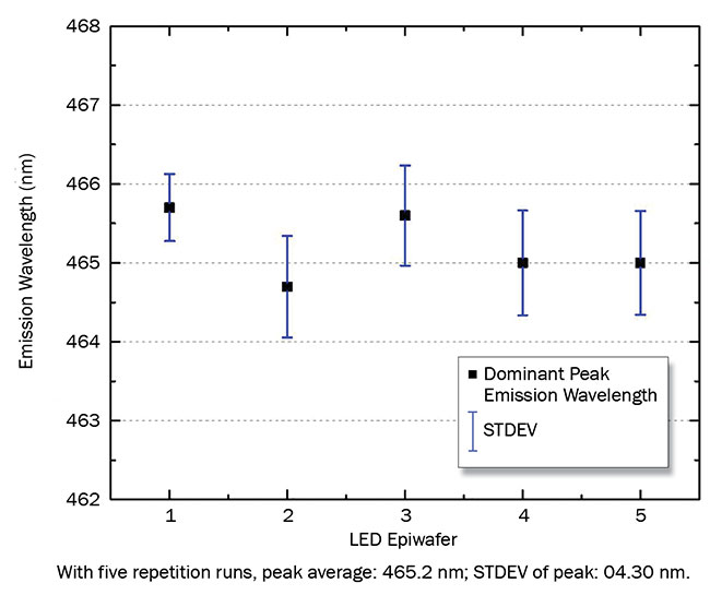
To meet visual performance requirements, peak emission of micro-LEDs must be uniform to within a few nanometers wavelength across a screen. Careful control of emission-layer thickness and post-processing allows for achieving the necessary performance. Here, micro-LED peak wavelength is uniform to within ±0.5 nm over multiple repeated runs.
“We take those regions of the source wafer and reconstitute them into a virtual wafer, which is now ultrauniform. And then we do a wafer-scale transfer,” Paranjpe said. In other words, chip repair is effectively achieved not at the end of the process but along the way. This approach improves yield and manufacturability.
With further innovations, and by working out the remaining processing hurdles, micro-LED displays could soon enter production, offering benefits at each end of the screen-size spectrum. Their low power consumption will benefit mobile applications. And Paranjpe said micro-LEDs can compete on cost with currently available large-screen alternatives, such as OLEDs, while offering increased brightness and equal or better color quality to the largest consumer-grade displays, such as TVs that measure more than 75 in. across.
Plessey Semiconductors of Plymouth, England, brings another example of what’s possible in the near future. The company’s GaN-on-Si micro-LEDs for augmented reality (AR) applications deliver 7× greater light output, 5× better contrast, and improved resolution compared to displays for similar applications that are based on LEDs or OLEDs, according to the company. Plessey demonstrated the technology in January at the Consumer Electronics Show (CES) in Las Vegas.
According to Mike Lee, Plessey’s president of corporate and business development, the advent of micro-LED displays will lead to a shift in technology as big as the switchover from cathode-ray tubes (CRTs) to LCDs. The change will lead to a rollout of smaller and less power-hungry devices, he said in a release announcing the company’s selection as a CES 2019 Innovation Awards honoree.
Nothing less than perfection
To solve micro-LED display manufacturing challenges, Plessey partnered with EV Group (EVG) of Sankt Florian am Inn, Austria. EVG specializes in wafer bonding equipment, the type of gear needed to transfer many thousands of micro-LEDs in a single batch directly onto a display or a silicon backplane. Having this capability would help cut the manufacturing costs of producing high-resolution micro-LED displays.
A wafer bonder enables transfer of micro-LEDs directly from a source substrate to a backplane. This may be necessary for large displays, which could require tens of millions of micro-LEDs.
The alternative is to complete the transfer via a pick-and-place process, said Thomas Uhrmann, EVG business development director. However, the micro-LED chips may only measure 20 to 30 μm on a side. Reliably picking up such tiny objects and then moving them without failure to a backplane presents a challenge. Anything less than perfection could result in a dead pixel, and this possibility goes up as the micro-LED becomes smaller.
“You have something as small as 3 or 4 µm that you detach from a source substrate and you temporarily hold it in a transfer gripper. Then you have to detach it in a controlled way and bond it,” Uhrmann said. Thus, the best solution may be to use a wafer-level process, with all the chips on a wafer being attached to the backplane at once.
An alternative to the direct-emission micro-LED display is known as the projection approach, in which a blue micro-LED is down-converted to create red or green light. This process offers the advantage of high-emission uniformity because quantum dots are used to down-convert the incoming blue light into a very precise red or green. And because the image is projected, it appears larger than it is. Projection micro-LEDs are being rolled out in AR applications and could show up in other places, such as in microprojectors.
With further innovations, and by working out the remaining processing hurdles, micro-LED displays could soon enter production, offering benefits at each end of the screen-size spectrum.
Since down-converting requires the laying down of a quantum dot or other down-conversion layer, the system must prevent blue light from leaking through into the red or green pixels. The layer absorbs and converts the blue light into red or green at specific locations. Given constraints on the thickness of down-conversion layers, leakage can be a problem. A waveguide must also direct the emission from each pixel into the projection engine.
Significant production of projection micro-LED displays may be only a few years away, according to Uhrmann. Direct-emission display will come further out because of the manufacturing challenges of repeatedly producing millions of narrow-wavelength micro-LEDs and assembling them into a final product.
According to Yole’s Virey, if these problems can be solved, production of micro-LED displays could reach over
300 million units by 2025. But it will likely take several years before mass production begins.
“We believe it will be at least another three to four years until we might see high-volume consumer products on the market,” Virey said.
[email protected]