An automated microfluidic technology has been developed containing a spectrographic monitoring module that collects both fluorescent and absorption data. The module moves along the microfluidic channel, collecting data along the way. The technology is capable of collecting 30,000 unique samples per day in both single and multi-phase flow formats.
Researchers believe that the technology could expedite the discovery, screening and optimization of colloidal semiconductor nanocrystals, such as perovskite quantum dots, by two orders of magnitude. Additionally, use of the technology revealed that the speed of mixing ingredients for quantum dots used in LEDs led to changes in the color of light the QDs emitted, even when all other variables were identical.
Researchers at North Carolina State University developed the modular, automated microfluidic platform for the systematic study of room-temperature synthesized cesium–lead halide perovskite nanocrystals.
“Semiconductor nanocrystals are important structures used in a variety of applications, ranging from LED displays to solar cells. But producing nanocrystalline structures using chemical synthesis is tricky, because what works well on a small scale can’t be directly scaled up — the physics doesn’t work,” said professor Milad Abolhasani.
Researchers have discovered that the speed of mixing ingredients for quantum dots used in LEDs changes the color of light they emit — even when all other variables are identical. Courtesy of Milad Abolhasani.
“This challenge has led to an interest in continuous nanomanufacturing approaches that rely on precisely controlled microfluidic-based synthesis,” he said. “But testing all of the relevant variables to find the best combination for manufacturing a given structure takes an extremely long time due to the limitations of the existing monitoring technologies — so we decided to build a completely new platform.”
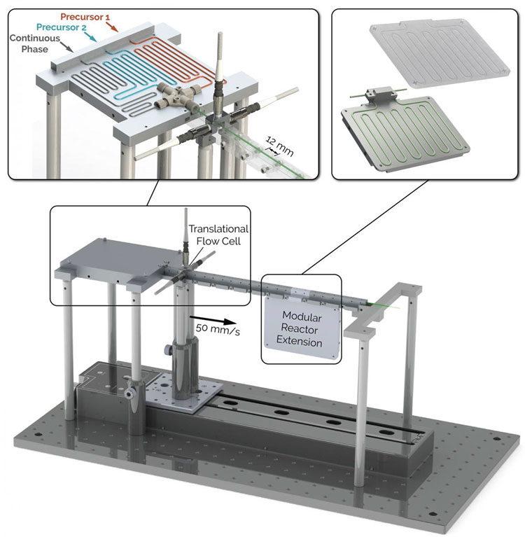
The researchers developed a high-throughput screening platform that features a custom-designed three-port flow cell with translational capability for in situ spectral characterization of the in-flow synthesized perovskite nanocrystals along a tubular microreactor. The translational flow cell allows for sampling of twenty unique residence times at a single equilibrated flow rate. The technique requires an average total liquid consumption of 20 μL per spectra and as little as two μL at the time of sampling.
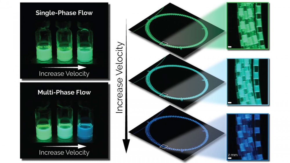
Researchers studied the growth of perovskite nanocrystals through in situ monitoring of their absorption and emission band-gaps at residence times ranging from 100 milliseconds to 17 minutes. The automated microfluidic platform enabled a systematic study of the effect of mixing enhancement on the quality of the synthesized nanocrystals through a direct comparison between single- and multi-phase flow systems at similar reaction time scales.
The automated NanoRobo system allows users to collect 100 times more spectrographic information per day from microfluidic devices, as compared to the previous industry standard. Courtesy of Milad Abolhasani.
The technology, called NanoRobo, allowed researchers to monitor reaction time and flow rate as separate variables. This led the team to discover that the speed of the samples in the microfluidic channel affected the size and emission color of the resulting nanocrystals. Even if all the ingredients were the same, and all of the other conditions were identical, samples that moved and mixed at a faster rate produced smaller nanocrystals, which afftected the color of the light they emitted.
The mixing characteristics of the multi-phase flow format resulted in high-quality perovskite nanocrystals with kinetically tunable emission wavelengths.
Further application of this novel platform could allow rapid parameter optimization in the colloidal synthesis of a wide range of nanomaterials (e.g., metal or semiconductor) for use in continuous manufacturing.
"This is just one more way to tune the emission wavelength of perovskite nanocrystals for use in LED devices," Abolhasani said.
North Carolina State University has filed a provisional patent covering NanoRobo and is open to exploring potential market applications for the technology.
The research was published in Lab on a Chip (doi: 10.1039/C7LC00884H).
NanoRobo is a fully automated microfluidic platform for discovery, screening and optimization of colloidal nanocrystals. Courtesy of Milad Abolhasani.