The tools and techniques that scientists and engineers need will continue to mature.
Jason Mulliner, National Instruments Corp.
Despite the less than stellar performance of recent years, the outlook for photonics looks bright. New technologies offer the promise of lower-cost bandwidth and simplified communications for consumers and businesses. The leading technology in this trend is miniaturization. Nanotechnology and microelectromechanical systems (MEMS), once the fodder for science fiction, have become a reality and will continue to push the unit of measurement for photonic devices to submicron levels.
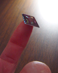
This eight-channel micro-optoelectromechanical chip is an example of the tiny photonic devices that offer new challenges in testing. Developed by Xerox Corp., it measures only 2 × 1.5 cm but can fit up to 24 functions. Courtesy of John Griebsch.
The wonders of miniaturization have been apparent over the past 20 years as more computing power is being crammed into tighter spaces. The result continues to be smaller electronic devices such as cell phones and notebook computers. Of course, as these content-client devices become more accessible and pervasive, the need for bandwidth will grow.
The progress toward miniaturization continues with the advent of MEMS. These tiny systems made headlines several years ago as the promise of all-optical communications networks materialized. Unfortunately, the expected benefits of MEMS to these networks were not realized. Today, MEMS are employed in such diverse applications as accelerometers in air-bag sensors, microfluidics for drug discovery and microdetectors for environmental analysis. As they mature, photonics applications will be able to leverage the technology to reduce size and costs and to improve performance.
Automation and testing
While sizes shrink and applications for new devices grow, software for automation and testing becomes increasingly powerful and more flexible, allowing designers and engineers to build complex systems using off-the-shelf PC-based components. This not only lowers the cost of systems, but also shortens the time to market — a definite advantage in the nimble and competitive world of photonics.
Software is the core of any test and automation system. Now more than ever, engineers can choose from a wide variety of software environments to solve problems in their applications. Configuration-based software packages do programming, and aid in optics design, machine vision inspection and motion control. In addition, tools for all types of automation are available in common application development environments such as C, C++ and LabView.
The photonics industry encompasses so many application areas that often it is difficult to use a general programming environment for all the requirements of a single application. But most of these environments have tool kits to provide add-on functionality and increased power, whether it be for machine vision, motion control or signal processing.
As the gap between software and hardware shrinks, technologies such as field-programmable gate arrays are becoming common on many devices used for testing and control of photonic equipment. Programming these arrays has typically required the knowledge of a hardware descriptor language. Graphical programming environments such as LabView allow the user to graphically create the hardware configuration that will run on the field-programmable gate array, thus speeding up the array’s control development and resulting in optimized closed-loop control of photonic equipment.
Whether it is the continued hardware miniaturization of devices with MEMS or the increased power and flexibility of software used for programming and testing, the tools and techniques available to photonics scientists and engineers will continue to grow and mature.
Meet the author
Jason Mulliner is machine vision product manager at National Instruments Corp. in Austin, Texas.