Engineering researchers at the University of Arkansas received $17.87 million from the NSF to build and operate a national silicon carbide research and fabrication facility. The unique and open-access facility at the university will serve to fill a gap in U.S. production of integrated circuits made with silicon carbide, a semiconductor suited for higher temperature environments.
Silicon carbide has long been studied, but efforts to use it as a fully developed semiconductor have been stunted by the lack of availability of high-quality silicon carbide wafers. Currently, all silicon carbide fabrication facilities in the U.S. are for internal use only. U.S. research and development of silicon carbide integrated circuits relies on international fabrication.
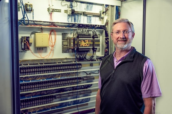
Alan Mantooth will lead the team of engineering researchers who will use a new $18 million, NSF-funded SiC research and fabrication facility in Ark. Courtesy of the University of Arkansas.
The facility, to be located in Fayetteville, Ark. will provide domestic opportunities for prototyping proof-of-principle demonstrations and device design. It will be the only openly accessible fabrication facility of its kind in the U.S., meaning its facilities and services will be available to external researchers.
“The national impact of having a fabrication facility such as this is enormous,” said distinguished professor Alan Mantooth, who will lead the engineering research team. “The country that leads the world in advancing silicon carbide semiconductor design and fabrication will also lead the race to market nearly all new game-changing technologies, including those used by the military, as well as general electronic devices that are essential to our economy.”
The NSF funding will pay for infrastructure, equipment, technology installation and enhancements to current facilities to accommodate new equipment. The funding will also cover three full-time staff members, a post-doctoral researcher for four years, and miscellaneous funds for setup and equipment operation.
Students at all degree levels will be given research opportunities and be exposed to a high-need area of science and technology. The research will also engage underrepresented students.
Co-principal-investigators on this project are Greg Salamo, distinguished professor of physics; Zhong Chen, associate professor of electrical engineering; Shannon Davis, business and operations manager in the Department of Electrical Engineering; and John Ransom, director of silicon carbide technology at X-FAB in Lubbock, Texas.