A new type of silicon metamaterial that has unique characteristics and is easy to manufacture promises a new direction in the development of metamaterials and their practical application to nano-optics and solar cells.
Researchers from the National University of Science and Technology
(NUST) MISIS have demonstrated a novel way to manufacture metamaterials by
perforating holes in the thin film of silicon or other dielectrics using
a focused ion beam (FIB). They found that an FIB can create holes up to
5 nm in size.
The result is a dielectric metamaterial that would support the anapole mode without 3D geometry and could be processed in one step using nanofabrication methods. Anapole is a non-emitting diffuser transparent to electromagnetic
radiation and is an ideal resonator.
Dielectric metamaterials can be used to control resonance in the optical spectrum. When irradiated from the outside,
anapole retains all the energy inside itself, while the electromagnetic
oscillations fade slowly. Compared to metallic metamaterials, dielectric metamaterials do not heat
under exposure to electromagnetic radiation, which minimizes their
energy dispersion.
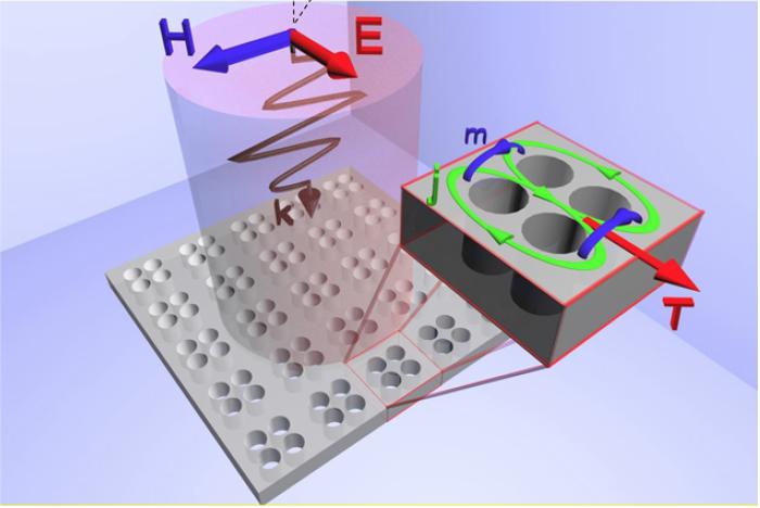
At right, the suggested metamaterial, wherein m designates magnetic dipole moment, j designates electric current loops, and T designates toroidal dipole moment. Courtesy of NUST MISIS.
“In the theoretical part of the experiment, we were able to
show that in the optical frequency range it will be possible to excite a
special anapole condition, which is promising for the strong
localization of electromagnetic fields, as well as sensors,” lead
researcher Alexey Basharin said.
Basharin suggests that, beyond the theoretical, "Real experiments with silicon should show the evidence of our technique and significantly increase the transparency of silicon plates, for example, for use in solar batteries." Basharin said.
The research was published in Laser & Photonics Reviews (doi: 10.1002/lpor.201800005).