Ana González and Antonio Raspa, European Photonics Industry Consortium (EPIC)
The increasing data traffic that has been stimulated by emerging services such as data center cloud services and 5G will require the use of technologies that can reduce power consumption, are cost-effective, and provide enhanced data security. In this context, the miniaturization provided by photonic integrated circuits (PICs) — small waveguides with nanometric dimensions — makes them the perfect technology to help achieve these results because they are fabricated on wafers using a standard complementary metal oxide semiconductor (CMOS) fabrication process. Additionally, lasers and other functions can be added by using indium phosphide (InP) PICs and/or other hybrid technologies in components, achieving all the necessary functions in a miniaturized, single platform.
Several main technologies are available based on PICs and other nanometric structures for optical communications applications in data centers, 5G, and quantum computing. However, challenges remain that need to be addressed to enable PIC technologies to fulfill their potential in these applications.
Manufacturers currently fabricate PICs on a variety of waveguide platforms, including InP, silicon nitride (SiN), silicon carbide, and lithium niobate, as well as glass and various polymers. Because each material has its advantages and disadvantages in the specific applications in which it is used, different PIC foundries have come to prefer particular waveguide materials. For example, LIGENTEC — a manufacturer of PICs for ground and space communications, as well as for quantum, lidar, and biosensor applications — focuses on SiN. In LIGENTEC’s view, SiN has important advantages over other platforms in these specialties, due to its low propagation loss, its ability to stabilize temperature, and its usefulness for dispersion engineering and for the ability to carry multiple watts of optical power per waveguide. Moreover, SiN is already employed as a material in CMOS foundries and can be efficiently scaled to high-volume production.
In contrast, the Fraunhofer Heinrich Hertz Institute (Fraunhofer HHI), a major European organization involved in photonics integration, has a foundry dedicated to the fabrication of InP PICs for both research and industrial use. For Fraunhofer HHI, the advantages of InP over SiN and other platforms include the following:
• Complex structures containing lasers, amplifiers, detectors, gratings, and waveguides can be integrated in a monolithic process.
• InP is a more developed technology; therefore, engineers are more experienced with it than with other platforms.
• With PICs, InP (a relatively expensive semiconductor material) can be used very efficiently with active and passive optical functions. In addition, the integration effort of the hybrid systems — which is otherwise required when integrating different functional components — is eliminated.
• Because established and detailed design kits are available, people with limited knowledge of photonics can design their own PICs after only a couple weeks’ training.
Both LIGENTEC and Fraunhofer HHI are working to integrate different PIC platforms with various technical characteristics to expand future capabilities.
Photonics in datacom
To meet the growing demand for data created by 5G, the Internet of Things, and cloud and streaming video, many data centers are upgrading their networks to 400-Gbit/s optical links using PIC technology. Compared with electronic integrated circuits, PICs have several advantages, including lower power consumption, much higher frequency coverage, and greater efficiency. Furthermore, in combination with III-V materials, silicon substrates are being used to fabricate hybrid PICs that generate less heat, provide greater electronic mobility at room temperature, and allow faster transfer of electrical currents through silicon semiconductors.
For these reasons, PICs have shown significant benefits for data centers and cloud computing by enabling simpler, more reliable, and higher-bandwidth communications. An example of a company that is providing PIC-based transceivers for data centers is HG Genuine, which offers a range of pluggable transceivers from 100G to 800G. However, although several new PIC-based processes have recently been brought to the data communications market, several challenges remain for the transceivers’ full implementation.
First, PIC-based devices are not necessarily lower cost per bit compared to VCSEL-based multimode solutions, especially when foundry costs and other investments are taken into account. Second, concerns remain over the power and reliability of the laser. In this respect, it is important to note that the operating condition in data centers is generally
45 °C ambient with evaporative cooling — meaning that PICs have to operate at 70 °C in 100% humidity, almost drenched in water. Third, many of the components come from a single source, and accepted best practice is now that devices must be produced in at least two geographic regions to ensure a strong supply chain. This lesson was learned with the recent pandemic that disrupted many industries. Finally, there is a lack of testing for possible burn in — an effect in which a shadowy image becomes permanently visible on a display — along with warranty coverage in the event that the effect occurs. All of these facts together indicate that the ecosystem still needs to evolve and grow to make data speeds beyond 400G a reality.
Photonics in 5G
Until now, the majority of data connectivity has been provided by microwave. However, all of the big network providers — such as BT Mobile, Ericsson, and Verizon — are currently investing heavily in rolling out optical fiber for connectivity between the antenna and the base unit. The advantages of fiber are low loss, large capacity, and (unlike with microwave) immunity to any kind of distortion, electromagnetic interference, or adverse weather conditions.
Examples of new enabling optical technology for 5G transport include self-tunable, multivendor interoperable, bidirectional dense wavelength division multiplexers (DWDMs). These devices increase bandwidth over existing fiber networks by combining and transmitting multiple signals simultaneously at various wavelengths on the same fiber.
Also important are bidirectional, “gray” point-to-point devices for connectivity between antennas over very short distances (<2 km); 400G coherent optical interfaces for short distances (<20 km); and high-speed (50G to 200G) direct-detection optical interfaces.
As with datacom, integrated photonics is playing a crucial role in enabling this new generation of low-cost, high-speed, tunable, and small-form-factor technology. An example of a company developing PIC-based devices for 5G is PICadvanced (Figure 1). The company currently provides a range of pluggable NG-PON2 (next-generation passive optical network 2) transceivers that supports a data rate of 10 Gbit/s. These devices come with a standard interface for small-cell base stations and can directly feed common routers with PON ports.
Figure 1. A PIC-based device for NG-PON2 applications. Courtesy of PICadvanced.
Quantum computing
Whereas conventional computers use binary bits that are either zero or one, quantum computers use qubits that, prior to measurement, can be both zero and one. This enables quantum processors to store an enormous amount of information and achieve processing speeds that are significantly faster than those of conventional computers, with potential applications such as performing powerful simulations. This capability is especially relevant in pharmaceutical and drug creation, banking, and e-mobility.
In the field of photonic quantum computing, photonics companies are currently developing two types of devices: qubit emitters and quantum processors.
Quandela is developing plug-and-play qubit emitters, designed around quantum dot-based single-photon sources, that emit photonic qubits. The qubits can be inserted into an optical fiber connected to a quantum processor to enable quantum computing (Figure 2). The company has also produced the world’s first fully commercially available quantum random number generator based on PICs with sources that are based on compact semiconductors only a few microns in size. The device emits a lineal stream of single, high-quality photons that can be sequentially entangled to generate cluster states in a matter of hours rather than years, as is the case when using a laser.
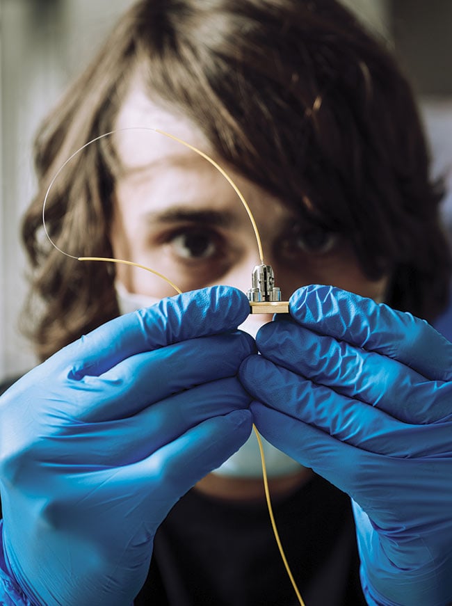
Figure 2. A plug-and-play photonic qubit emitter. Courtesy of Quandela.
An example of a quantum processor developer is QuiX, a spinoff of the University of Twente. The company’s main product is a quantum photonic processor, which is basically a reconfigurable photonic chip in the form of a large-scale tunable interferometer that is very stable and capable of scaling (Figure 3). This processor has three main properties. First, it is low loss, as low as 0.1 dB per centimeter, thanks to the SiN waveguides. Second, it is also plug and play, as it comes with a seamless integration of the dedicated control software. Finally, it is fully reconfigurable, resembling a sort of multipurpose, off-the-wall field-programmable gate array.
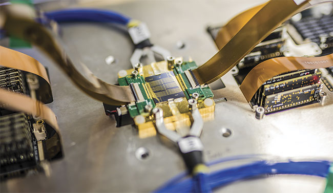
Figure 3. A quantum photonic processor. Courtesy of QuiX.
The use of the SiN platform also provides a wide transparency window, from 400 nm to 3.7 µm. This means that the processor can be interfaced with all common single-photon sources — including, for example, commercially available quantum dots, nonlinear crystal, and spontaneous parametric downconversion sources. The applications of the photonic processors developed at QuiX are various and include quantum information processing, quantum chemistry, and machine learning.
Cybersecurity
The growing number of cyberattacks, together with the complexities of cyber risk management, are also driving the development of quantum-based data security solutions. Currently, sensitive data is typically encrypted and then sent across fiber-optic cables together with the digital keys needed to decode the information. Both the data and the keys are sent as classical bits — a stream of electrical or optical pulses representing zeros and ones.
But this makes classical encryption solutions vulnerable in two key respects. First, because the keys are based on random numbers generated by computer algorithms, the numbers are not truly random. They may seem random to the untrained eye, but if one knows the underlying algorithm, the numbers become completely predictable. This predictability means that attackers who are sufficiently patient and knowledgeable can crack almost any encrypted data that they want. The ever-constant increase in ransomware, cryptojacking, and DDoS (distributed denial of service) attacks testifies to this potential.
One way around this dilemma has been to move away from math and classical physics and take advantage of the unpredictable behavior of subatomic particles such as electrons and photons for the purposes of encryption. Since the 2000s, several commercial quantum random number generators have become available. These are based on the randomness of physical processing that results from quantum tunneling, the distribution of individual photons as they hit a detector, and fluctuations in the intensity of LED light.
Quside is working in this area. The company produces a quantum random number generator capable of generating raw random numbers at entropy bounds above 90% at 400 Mbit/s — much faster than other commercial devices currently operating at 40 and 240 Mbit/s. Quside’s phase-diffusion technology is based on InP PICs using a heterodyne interferometric configuration that can reach multiple-gigabit rates of quantum randomness generation.
The second problem with classical encryption is that, because the keys are sent in classical bits, a smart hacker can read and copy the bits without leaving a trace. The breach of data itself is bad enough, but there can be an enormous degree of anxiety during communication, because neither the sender nor recipient can become aware of the compromised information.
The issue has been addressed by using quantum communication in a process known as quantum key distribution (QKD). In this system, keys are sent in the form of qubits, and the main advantage — from a cybersecurity perspective — is that if a hacker tries to observe the data in transit, the superfragile quantum state of the qubits “collapses” to either zero or one, thus leaving a telltale sign of the activity. When this happens, both parties can ditch the suspect key and keep generating new ones until they are confident that they share a secure key.
Several companies are currently providing components and technologies for QKD networks, including ADVA, which provides 10G and 100G muxponders (a sender and receiver of multiple optical signals on a fiber). VPIphotonics developed a system-level model library for QKD. And Bay Photonics specializes in packaging design and assembly of prototypes of PICs used in quantum devices for secure communications in lidar and high-speed receive/transmit modules for datacom.
Progress continues
These challenges have not hindered progress. Over the last few years, the European photonics industry has made great strides in developing a robust ecosystem to support the growth of PIC-based technology not only in datacom, 5G, and quantum but also in other applications such as personal health, agrifood, the life sciences, and structural monitoring.
Instrumental in this push have been EPIC (the European Photonics Industrial Consortium) and the European Union (EU)-funded pilot lines. The JePPIX Pilot Line is dedicated to production of InP chips, offering design, manufacturing, and testing services. The PIXAPP Pilot Line offers services for packaging and assembly of these PICs. Finally, PHABULOµS offers pilot production of freeform micro-optics. These pilot lines are helping European small- to medium-size enterprises develop the tools and processes needed to scale up the manufacture of innovative PIC-based components by providing services for chip fabrication and standardized photonic packaging technologies.
In terms of size, weight, and functionality, PICs have several indisputable advantages over traditional technologies, as exemplified by the new generation of pluggable transceivers for datacom, DWDMs for 5G, and PIC-based quantum processors and random number generators. Although these technologies are still in development and many challenges remain, based on the progress made to date, there is every reason to believe that the PIC community will be able address the challenges and push PIC technology to center stage in multiple industries.
Meet the authors
Ana González, Ph.D., is R&D manager at EPIC (the European Photonics Industry Consortium). Her role is to understand the technologies developed by EPIC members and to identify potential collaborations among the organizations. González also participates in European Commission initiatives such as the various pilot lines in photonics for which she manages business development and marketing strategy. Her expertise lies in the development of optical systems and the investigation of applications such as sensing and datacom. She received her bachelor’s degree in chemistry from the Autonomous University of Barcelona and her doctorate from the Catalan Institute of Nanoscience and Nanotechnology.
Antonio Raspa is the innovation manager of EPIC and has a background in electrical engineering, with a specialization in quantum electronics. Before joining EPIC, he worked at Quanta System as R&D manager, developing solid-state laser sources and customized photonic systems for industrial and scientific applications. During the same period, he was also in charge as lidar specialist of the Italian research program in Antarctica. Later he worked at TRUMPF and Rofin-Sinar as an industrial laser products and processes specialist. In 2009, he again joined Quanta System, organizing and managing a brand-new structure to produce sterile optical fibers for surgery.
Acknowledgments
PIXAPP is the world’s first open-access PIC assembly and packaging pilot line. It has received funding from the EU’s Horizon 2020 research and innovation program under grant agreement No. 731954 (www.pixapp.eu).
The JePPIX Pilot Line democratizes access to industrial prototyping and preproduction of high-performance InP PICs. JePPIX is enabled by the InPulse project, which has received funding from the EU’s Horizon 2020 research and innovation program under grant agreement No. 824980 (www.inpulse.jeppix.eu).
PHABULOµS aims to strengthen Europe’s leading position as a technology and machine provider for the production of micro-optics based on a value selling model that retains the high-cost and high-value technology portfolio in Europe. The PHABULOµS Pilot Line has received funding from the EU’s Horizon 2020 research and innovation program under grant agreement No. 871710 (www.phabulous.eu).