Scientists at Tokyo Institute of Technology (Tokyo Tech) have generated low-cost extreme ultraviolet (EUV) light by creating tin thin-film spheres using a polymer electrolyte “soap bubble” as a template and irradiating it with a laser. When the spheres were irradiated, the scientists were able to confirm the emission of EUV rays of 13.5 nm, which is the same as metallic tin. The low-density tin “bubble” could provide a reliable way to generate EUV light for use in electronics, biotechnology, and cancer therapy.
High-intensity lasers have been used to generate EUV light, but it has been challenging for these lasers to maintain control of a target density that can produce light in the EUV range. Tin has been considered as an option, but its dynamics are difficult to control.
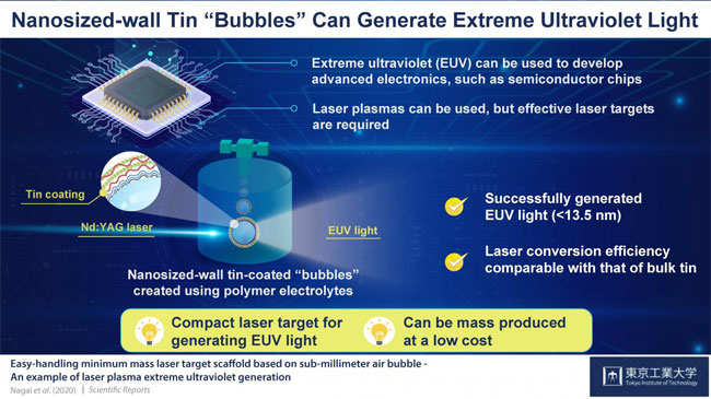
Nanosize-wall tin. Courtesy of Keiji Nagai.
The team from Tokyo Tech, working with colleagues from University College Dublin, set out to find efficient, scalable, low-cost laser targets that could be used to generate EUV. The scientists created a tin-coated microcapsule or “bubble” — a low-density structure weighing as little as 4.2 nanograms and with a high level of controllability. For the bubble, they used polymer electrolytes, which are a dissolution of salts in a polymer matrix. The salts act as surfactants to stabilize the bubble.
The scientists coated the bubble with tin nanoparticles. “We produced polyelectrolyte microcapsules composed of poly(sodium 4-styrene-sulfonate) and poly(allylamine hydrochloride) and then coated them in a tin oxide nanoparticle solution,” professor Keiji Nagai said.
To test the bubble, the scientists irradiated it using a neodymium-YAG laser. This resulted in the generation of EUV light within the 13.5-nm range. The team further found that the structure was compatible with the conventional EUV light sources that are used to manufacture semiconductor chips.
Laser conversion efficiency with the tin bubble matched that with bulk tin. “Overcoming the limitations of liquid tin dynamics can be very advantageous in generating EUV light,” Nagai said. “Well-defined, low-density tin targets can support a wide range of materials including their shape, pore size, and density.”
In addition to applications in electronics, Nagai is optimistic that the team’s technology could be used in cancer therapy. “This method could be utilized as a potential small-scale/compact EUV source, and [for] future quantum beam sources such as electrons, ions, and x-rays by changing the coating to other elements,” he said.
Polyelectrolyte bubbles are extremely stable soap bubbles and are suitable for mass production. Since the method can be applied not only to tin but to other elements in principle, it could be used to achieve a 6.x-nm light source. It could also be applied to targets such as existing carbon ion beams.
The team is seeking collaborators with large laser facilities in Japan and/or other countries.
The research was published in Scientific Reports (www.doi.org/10.1038/s41598-020-62858-3).