ROCHESTER, N.Y., June 28, 2019 — One of the many perks of attending the Light and Sound Interactive (LSI) conference is getting a tour of the AIM Photonics facility. The 30,000-sq-ft facility is located on the Kodak campus in Rochester, N.Y., and boasts state-of-the-art equipment for the testing, assembly, and packaging (TAP) of photonic components, and potentially electronics components, according to Ed White, associate vice president of the facility and chairman of the National Photonics Initiative.
A Kodak alumnus, White led the tours, sharing his expansive knowledge of the industry and the facility’s history.
To get some of the tools that the current facility uses into the building, one entire wall had to be removed to bring them into the cleanroom by a crane.
The tools were heavy enough to necessitate a load-spreading base to prevent them from falling through the floors and into the reception area, White said.
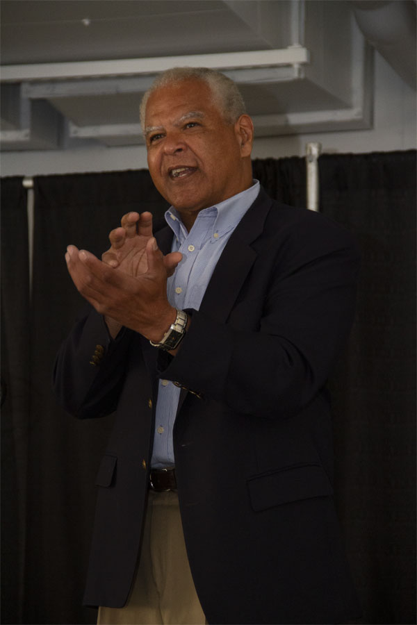
Ed White, Associate Vice President of the TAP facility and chairman of the National Photonics Initiative. Courtesy of Manon Mirabelli.
“Three-hundred-millimeter semiconductor tools are big; they’re heavy. To give you an idea, our litho tool 5520 Canon eyeline stepper: 23,000 pounds,” he said.
“Some of the tools are so precise, we’re taking a 10 µ — one-tenth the thickness of a human hair — trying to match it up with a 400- × 200-nm waveguide — so precise that we had to put vibration isolation in under some of those tools.”
The facility has four layers of security. Employees scan their badges on the first, fourth, and fifth floors to enter a cleanroom, and once more to operate a machine. The cleanrooms are connected with clean stairwells so employees don’t need to regown when traveling from room to room. Cleanrooms are lit with yellow light so as not to damage sensitive materials such as silicon wafers with UV light, White said. The fluorescent lights are fitted within yellow tubes to filter out the harmful UV portion of the spectrum, at about 350 to 360 nm.
The facility does a great deal of work with the U.S. Department of Defense and many large companies, and a fair amount of the specifics related to projects are protected under nondisclosure agreements. The facility enforces a strict no-cameras policy, and phones are to be kept in one’s pocket.
At present, AIM is seeking tenants to set up shop in the TAP facility. For more information on the facility and how to join, visit www.aimphotonics.com/tap-facility.