
New Optical Beamformer Designs Spotlight High-End Applications
The ubiquity of smart devices and the telecommunications networks on which they rely is raising demand for electromagnetic beamforming technologies. The wide range of applications that make use of beamformers can be grouped in two main domains, namely 3D sensing and communications.
Within the 3D sensing sector, light detection and ranging (lidar) is one of the dominant markets. Mainly propelled by assisted driving and autonomous vehicle applications, the overall lidar market is expected to grow from $1.6 billion to
$3.8 billion between now and 2025, according to a market report by Yole Développement. And lidar is expected to penetrate other markets, such as consumer devices, where it can support and enhance developments in augmented reality (AR) platforms.
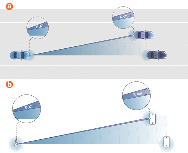
Whether a beamformer is applied in a lidar system to detect traffic and obstacles (a) or in a 5G network to accurately access a distinct mobile device (b), its ability to achieve accuracy at hundreds of meters requires an angular precision of fractions of a degree at the beamforming side. Courtesy of imec.
Apple was the first to integrate lidar functionality into its iPhones and iPads, setting a precedent for the mobile device market and leading competitors to follow suit. And more high-end applications are on track for development, such as medical devices for noninvasive monitoring of vital signs, or for dental or skin scanning. The technology is also finding applications in aerospace, such as topography analysis; earth observation; the monitoring of crops or soil; and high-resolution radar systems for target detection, tracking, imaging, and recognition.
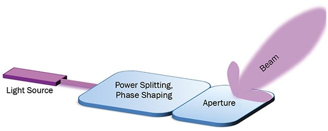
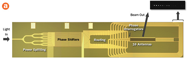
A schematic of a typical optical beamformer architecture. Courtesy of imec.
Electromagnetic beamformers are also finding application in telecom. The fifth- and sixth-generation mobile communications standards, 5G and 6G respectively, are among the most well-known examples of a wider set of high-bandwidth communication protocols that make use of directional antennas and beamforming technologies. The same applies to free-space communication such as satellite communications, avionics, and Li-Fi networks.
Pathways to development
While the opportunities for electromagnetic beamforming seem endless, further advancements are running into limits imposed by the need for cost-effective manufacturing, stringent user requirements, or the laws of physics. Whether the challenge is to allow lidar to detect traffic and obstacles, to enable an AR-equipped smartphone to deliver full-room scanning, or to permit a 5G network to connect with a distinct mobile device, there is a constant push to achieve higher resolutions and to perform over longer distances. Aiming for centimeter accuracy at tens to hundreds of meters requires angular precision down to fractions of a degree at the beamforming side.
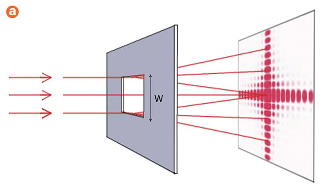
The aperture width (W) of a scanning system is directly related to the desired resolution for an application and the frequencies used (a). Consequently, beamformers are moving to higher frequencies in the pursuit of higher resolutions (b). Courtesy of imec.
Meeting such requirements with incumbent mechanical beam-steering
approaches would result in bulky and costly solutions. What’s more, such mechanical components are prone to suffer from reliability issues because of their sensitivity to mechanical shocks and vibrations. Consequently, both suppliers and end users are actively seeking fully digital systems that can eliminate all mechanically moving parts.
The search for improved resolution is further prompting the move toward
beamforming systems that are capable
of operating at higher frequencies. The system aperture is proportional to the
desired resolution, as well as the applied frequency. While lidar is already operating in the terahertz range, radar solutions are limited to a few tens of gigahertz, which would result in unrealistic apertures to obtain low angular resolution. With terahertz frequencies, similar resolutions can be reached using aperture form factors that are four orders of magnitude smaller.
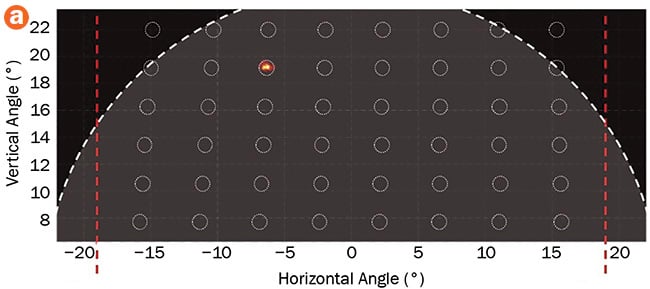
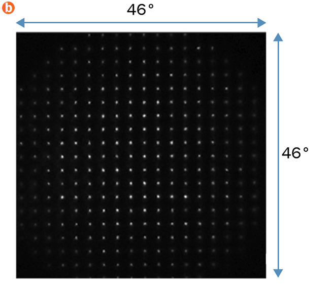
Demonstrations of 2D single-spot scanning lidar (a), and 2D steerable structured-light lidar (b). Courtesy of imec.
The smaller the form factor, the more easily a beamformer can be integrated and produced at acceptable price levels, especially if it is compatible with high-volume semiconductor manufacturing processes.
This is exactly why the state of the art in optical scanning systems is evolving
from the rotating arrays of lasers and
detectors currently available on the market to on-chip integrated photonics solutions that are increasingly appearing in prototypes and industry literature. The 2020 Consumer Electronics Show, for example, featured several examples of integrated silicon-photonics solutions for 3D scanning applications.
Conceptually, such integrated-photonics solutions use beamformers that consist of a waveguide, phase shifters, and an array of on-chip antennas (see schematic). Through controlled phase modulation, the antennas can transmit signals in a controlled direction. Notably, such on-chip systems are subject to inevitable manufacturing variations, which will cause inevitable deviations in the phase modulation and behavior of the system. To compensate for these inherent
aberrations, calibration is required. Normally, this process is performed in a controlled and complex optical setup after the devices are manufactured. The calibration protocol relies on making individual phase corrections afterward by pretesting the device under various signal conditions. This testing protocol, however, can be very impractical, both in terms of throughput (when many devices need to be calibrated) or in cases where recurring calibration may be needed.
More recently, a new integrated optical beamformer architecture has emerged to address many of these challenges. In the latest demonstrations, this beamformer design can cover a 40° field of view with angular precision below 0.2°, and these specifications leave room for further improvements aimed at market-ready implementations.
The main novelties of this solution
are in the architecture and the choice of
material platforms. Where typical solid-state lidar systems are built either in silicon or silicon nitride (SiN) photonics,
new beamformer designs combine both materials. They construct the waveguide and the antennas in SiN to allow for low-loss, high-power handling and good process control1. Conventional silicon photonics, meanwhile, comprises the phase shifters and on-chip photodetectors. Silicon photonics-based phase shifters have proven to be the preferred option over SiN platforms because they can achieve low-power compact operation. Steering at 2D is performed by the phase shifter via wavelength sweeping2.
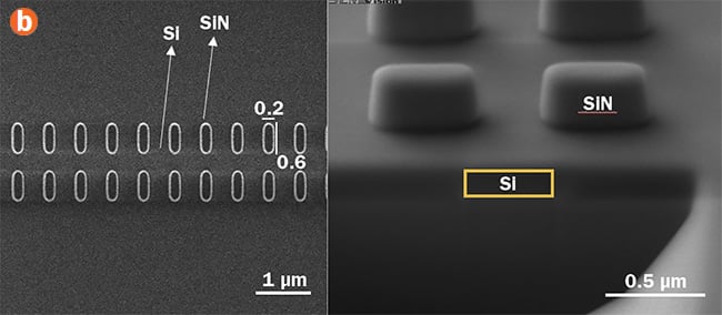
Optical beamforming chips (a) fabricated on imec’s 200-mm photonic pilot line are based on silico nitride-on-silicon technology for lidar applications. The scanning electron microscope image (b) shows top and side views of antenna elements.
Since the entire system is compatible with semiconductor manufacturing
flows, it can drastically reduce production costs in high-volume manufacturing processes. Similar on-chip technology from imec recently contributed to the field demonstration of a frequency-modulated continuous-wave lidar system3.
On top of its performance improvements and potential for low-cost manufacturability, the emerging beamformer solution self-calibrates via an on-chip solution. More specifically, it relies on
on-chip interferometers embedded in
between the phase shifters and the
antennas.
The interferometers assess the actual phase difference produced between two adjacent antennas. When measured with integrated photodiodes, the information provides an absolute indication of the far-field beam quality — for example, its direction and size — and compensates for aberrations before the signal gets transmitted.
The optical beamformer technology was recently used to steer structured-light with a 46° field of view in the vertical and horizontal directions4. These results indicate that the technology could pioneer a new generation of improved beamformer applications and help to expand the use of the components across a wider range of domains.
Meet the authors
Xavier Rottenberg is a fellow at imec; email: [email protected].
Marcus Dahlem is principal member of technical staff at imec; email: [email protected].
Philippe Soussan is program director at imec; email: [email protected].
Amin Abbasi is business development
manager at imec; email: [email protected].
References
1. J.Ø. Kjellman et al. (Feb. 25, 2020).
Silicon photonic phase interrogators for on-chip calibration of optical phased arrays. Proc SPIE, Vol. 11283, Integrated Optics: Devices, Materials, and Technologies XXIV, 112830X, San Francisco,
www.doi.org/10.1117/12.2546542.
2. W. Bogaerts et al. (2020). A 2D pixelated optical beam scanner controlled by the laser wavelength. J Sel Top Quantum Electron, Vol. 27, Issue 1, pp. 1-12.
3. A. Martin et al. (2018). Photonic integrated circuit-based FMCW coherent LiDAR.
J Lightwave Technol, Vol. 36, Issue 19,
pp. 4640-4645.
4. R. Jansen et al. (2020). Integrated calibration-free scannable structured light for fast high-resolution LiDAR. OSA Advanced Photonics Congress.
/Buyers_Guide/Imec/c22187