Although InGaAs sensors remain dominant in the big picture, SWIR detectors that employ quantum dots and innovative designs are starting to fill the frame.
HANK HOGAN, CONTRIBUTING EDITOR
Imaging in the shortwave infrared (SWIR) range, from 1000 to 2500 nm,
offers significant new advantages in an array of applications, from autonomous vehicles to food quality inspection.
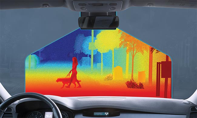
SWIR photons are scattered less by dust or fog than shorter wavelengths, allowing cameras operating in this spectral range to detect objects more easily. TriEye paired SWIR imaging with lasers emitting in the same range to develop a system that could also deliver image depth in adverse atmosphere conditions. Courtesy of TriEye.
SWIR photons are scattered less by dust or fog than shorter-wavelength light, for example, which allows cameras
operating in this range to provide visual data for advanced driver assistance systems and self-driving cars. Because wavelengths above 1400 nm are eye safe, SWIR systems can also use brighter illumination for tasks such as checking driver alertness.
In agriculture and food production, SWIR imaging can help to gauge
moisture content due to water’s absorption peaks at 1500 and 1900 nm. This capability provides a useful metric for
monitoring crop health or evaluating
food quality.
But all of these potential plusses come with one substantial minus: cost. The price for SWIR cameras today can run in the tens of thousands of dollars, which is too expensive for many applications and has inhibited wider use of the technology.
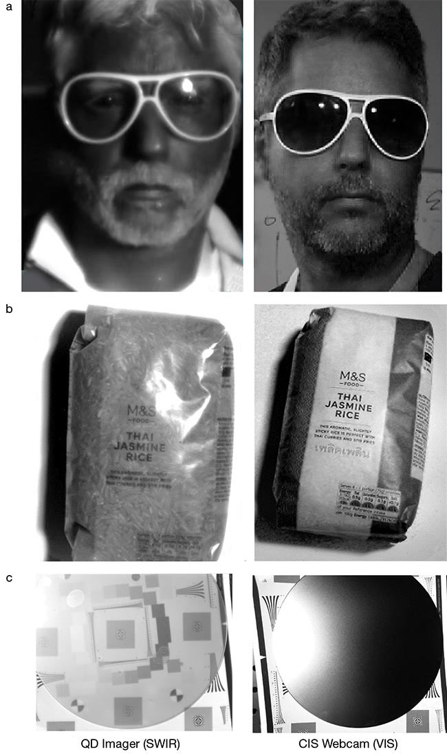
Cameras that sense wavelengths between 1000 and 2500 nm can often pick up details that would otherwise be hidden in images captured by conventional CMOS image sensors (CIS) that operate in the visible range. SWIR cameras can not only view details obscured by plastic sunglasses (a) and packaging (b), they can also peer through silicon wafers to spot voids after the bonding process (c). QD: quantum dot. Courtesy of mec.
“By lowering the price by an order of magnitude or more, you can open up whole new applications outside of labs and the military,” said Matthew Dyson, a senior technology analyst at the emerging technology consultancy IDTechEx.
Silicon, the dominant sensor material
for visible imaging, does not absorb SWIR photons without surface modification — and even then, it performs poorly. As a result, most SWIR cameras today use sensors based on indium gallium
arsenide (InGaAs), which produces 80, 90, or more photoelectrons for every
100 incoming photons. The compound semiconductor’s high quantum efficiency can apply across all SWIR wavelengths by altering the composition of InGaAs.
Emerging SWIR sensor materials
produce fewer photoelectrons, and hence a smaller signal per photon. Consequently, Dyson predicts that, for the foreseeable future, InGaAs sensors will continue to prevail in applications for which performance is paramount. In end uses for which performance is a secondary consideration, sensors based on colloidal quantum dots (QDs) are gaining interest. The technology uses nanocrystals made of semiconductor materials, such as lead sulfide (PbS), that absorb in the SWIR. By adjusting the size of the nanocrystals
used, sensor fabricators can create photodetectors that are sensitive from the visible to 2000 nm or even longer wavelengths.
A few years ago, the quantum efficiencies of such photodetectors were below 20%. But performance has steadily improved with the underlying materials
and processing science, according to Pawel Malinowski, program manager of pixel innovations at imec. The organization’s third-generation QD-based image sensor debuted a couple of years ago with an efficiency of 45%. Newer sensors have delivered above 60% efficiency.
SWIR Vision Systems focused the development of its imagers on a colloidal QD approach because the technology allows inexpensive and high-volume manufacturing, according to the company’s CTO, Ethan Klem. One reason is that QDs do not demand the intensive processing needed to produce InGaAs or silicon sensors.

A SWIR imaging forecast shows emerging
sensor materials taking a larger share of the market, while incumbent InGaAs sees little gain, and the use of other materials grows at a faster rate (top). OPD: organic photodetector. Courtesy of IDTechEx.
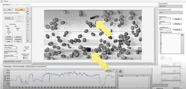
SWIR imaging can detect otherwise difficult-to-spot contaminants in coffee beans (bottom). Imaging capabilities in the SWIR offer further advantages in industrial, farming, and medical applications. Courtesy of Princeton Infrared Technologies.
“The material system itself is very
low cost to begin with because of the way the semiconductors are synthesized
in a chemical solution-type process that looks like the production of paint,” he said.
Fabricating QD photodiodes and sensors is also inexpensive because the sensor stack consists of a QD layer a few hundred nanometers thick, along with conducting, structural, and protective layers, Klem said. The stack goes atop a CMOS readout circuit in a pixel array. The technique can accommodate high-volume manufacturing processes and produce either large or small pixel arrays. Compared to InGaAs technology, QD sensors offer higher resolution and lower noise levels, along with fast response times.
SWIR Vision Systems aims to lower the cost of its sensors enough to make them viable additions to cars and mobile phones — markets that demand millions of units a year. Machine vision suppliers and industrial end users will also benefit from these lower costs.
Emberion, a startup spun out of Nokia, also makes QD-based SWIR cameras
and plans to eventually offer easy-to-
integrate camera cores, said Jyri Hämäläinen, the company’s head of product management. One advantage to Emberion’s fabrication method is that it gives QD sensors a broad dynamic range that prevents saturation when light levels vary. This capability allows the company’s cameras to capture details in bright or dark illumination over a spectrum that ranges to 2000 nm.
The quantum efficiency of these sensors is only 20% at 1800 nm. But Hämäläinen said Emberion’s QD sensor performance is competitive with InGaAs devices at that wavelength. “We can
compensate for the slightly lower efficiency with lower noise in our [readout] IC,” he said.
Another approach for the company to address the low quantum efficiency of its sensors would be to alter the mix of nanoparticle sizes, which would change the quantum efficiency at selected wavelengths — perhaps even doubling it in some cases.
With Emberion’s current technology, the company offers cameras with superior features at about half the price of InGaAs-based systems, according to Hämäläinen. As with other QD camera suppliers, he said, industrial and agricultural uses show promise. But Emberion is also viewing potential medical applications, for which SWIR imaging offers new ways to detect skin cancer, spot infections, and identify tooth decay.
Illuminating innovations
Imec is concentrating its research and development efforts on sensors operating
at eye-safe wavelengths between 1400 and 1550 nm, a spectral range that Malinowski said is attracting the most market attention. Along with further
sensor innovations, he cited a growing
demand for improved illumination. Halogen lamps, while effective, are both inefficient and large. Instead, illumination developers are working on SWIR laser chips, which he said could be integrated with SWIR sensors to create compact and sophisticated imaging solutions.
In December 2021, for example, SWIR camera-maker TriEye announced a
partnership with a VCSEL-maker that would enable a SWIR-based imaging
and depth-sensing system. Potential
applications include industrial automation, mobile phones, and automotive.
TriEye has been secretive about the technology underlying its sensor. When asked, senior product director David Cheskis said only that the material platform is based on CMOS.
Academic papers co-authored by one of the company’s founders around the time that TriEye came into existence discuss pyramid-shaped silicon nanostructures that detect SWIR photons via plasmonic enhancement of internal photoemission. The detectors described consist of silicon and CMOS-compatible metals.
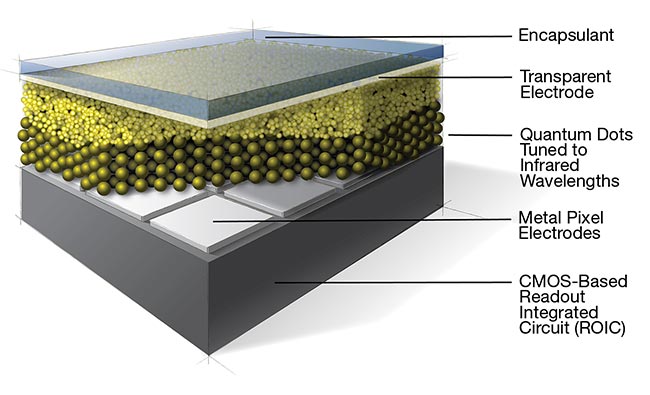
Quantum dots (top) act as a SWIR photodetector if they are sized correctly. When placed on a readout circuit, they form a SWIR imaging sensor.
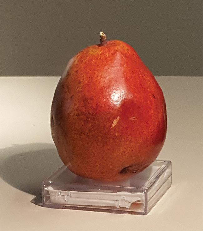
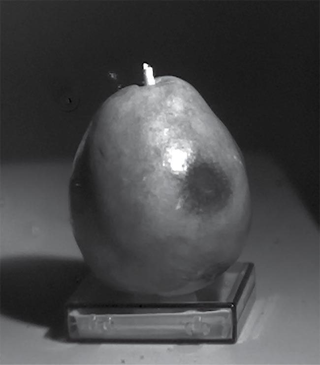
Water’s spectral absorption peaks at 1500 and 1900 nm make it comparatively easy to reveal cellular damage where moisture concentrates in bruised fruit. The bruise on the pear is virtually indiscernible in the visible image (middle), whereas it is evident in the image captured with a SWIR camera (bottom). Courtesy of SWIR Vision Systems.
Whatever its mechanism of operation or construction, TriEye’s photodetector is currently a 1.3-MP imager that detects wavelengths to 1600 nm. Cheskis said the company’s fabrication method costs as much as 100× less than the methods that produce InGaAs cameras. This low-cost production approach is key to TriEye’s business strategy, which targets automotive applications. The potential market could support tens of millions of units annually.
Using active illumination could
improve the performance of TriEye’s sensor. However, combined with the right light source, the sensor could enable the company’s Spectrum Enhanced Detection and Ranging (SEDAR) platform.
“With proper illumination in the SWIR range, it allows us to do simultaneous SWIR HD imaging plus deterministic depth sensing at the pixel level,” Cheskis said.
IDTechEx’s Dyson said organic
photodetectors on top of silicon readout chips are another possible SWIR imaging technology. Extending the response curve of the organics into the SWIR range requires using challenging chemical synthesis methods, however, so it may be years before the technology becomes commercially competitive, if it ever
does.
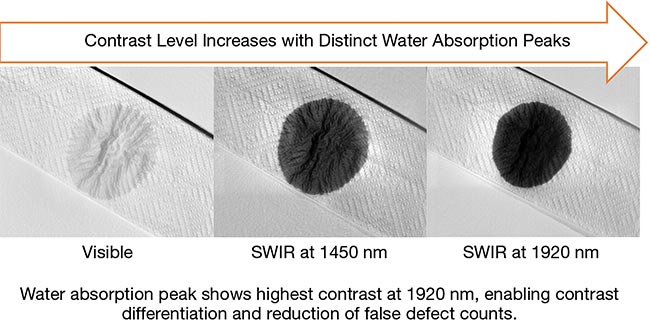
Due to water’s high spectral absorption at SWIR wavelengths near 1500 and 1900 nm, it is easier to capture moisture in a high-contrast image. This is beneficial in applications such as food inspection and assessing crop health. Courtesy of Emberion.
Imec has explored using germanium-on-silicon readout chips to develop SWIR sensors, Malinowski said. Germanium offers an extremely fast response time but has a high dark current, which raises the noise floor because current is produced when no light shines on a pixel. Germanium may thus be suitable for applications that would benefit from fast response times and can tolerate its higher noise.
Reducing costs
A universal goal of imec, TriEye, and other SWIR developers is a two to three order of magnitude cost reduction in SWIR imaging. “The long-term game is to get to double-digit or single-digit [dollar] cost per sensor,” Malinowski said. Quantum dot-based sensors could achieve this price point if production volumes are high enough.
Vendors of InGaAs solutions are undertaking their own plans to cut costs, improve performance, and expand markets. Martin Ettenberg, president and CEO of InGaAs camera-maker Princeton Infrared Technologies, said newer formulations of the SWIR-sensitive material InGaAs and of gallium arsenide antimonide that are lattice matched to the indium phosphide substrate on which the detector sits enable absorption in the extended SWIR. The company has a 1.3-MP product that
senses to 2100 nm, for example. He said that employing larger substrate wafers and wafer scale processing of the hybrid-
ization step that brings InGaAs and a readout integrated circuit together will significantly reduce the future price per sensor.
Thus, emerging materials such as QDs may cut costs and expand markets. But they will not do so without competition from incumbent InGaAs technology.