Fast low-noise electronics and lasers have enabled recent advancements in quantum sensing technologies.
NIKLAS WAASEM, HÜBNER PHOTONICS; HELMUT FEDDER, SWABIAN INSTRUMENTS; AND PATRICK MALETINSKY, UNIVERSITY OF BASEL
Sensors form an important foundation for many everyday devices, including microphones, CCD cameras, and touch sensors in smartphone displays. Moreover, sensors play a key role in technological progress, in general, as illustrated by the old adage that says “what you cannot measure, you cannot improve.” Consequently, progress in engineering, science, medicine, and other disciplines often relies on the development of new or improved sensing techniques.
Sensors typically rely on physical, chemical, or biochemical effects that transform a measured quantity into an electrical signal. Employing quantum effects opened a toolbox of new sensing methods and enabled the first so-called quantum revolution in the 20th century for technologies such as nuclear magnetic resonance spectroscopy, magnetic resonance imaging, and the development of transistors, LEDs, solar panels, and lasers.
Today, we are in the middle of a second quantum revolution that builds on the control and detection of individual quantum states in microscopic systems such as atoms, quantum dots, and color centers. Emerging quantum sensing techniques could lead to the improvement of multiple sensing technologies, ranging from sensitive quantum gravitometers, accurate atomic clocks, and low-noise quantum interference microscopy.
Another example of a quantum sensing technology that has matured over the last several years is nanoscale magnetometry using nitrogen-vacancy (NV) centers in diamond. These centers act as optically addressable, highly sensitive quantum sensors that are localized to atomic length scales. Using a scanning-probe approach with one NV center at the tip of an atomic force microscope cantilever allows measurement of magnetic fields with a spatial resolution on the nanometer scale and an absolute precision >1 µT/Hz1/2.
The demonstration of new quantum sensing techniques and subsequent development of quantum sensing products both rely on the availability of state-of-the art components such as specialized diamond tips,
suitable microscopy hardware, fast low-noise electronics, and high-performance lasers.
Nanoscale quantum magnetometry
Over the last decade, single-electron spins in diamond have been established as nanoscale quantum sensors that exhibit excellent sensitivity and nanoscale resolution for imaging and sensing of magnetic fields and other quantities, such as electric fields or temperature. Spins couple naturally to magnetic fields through the
Zeeman effect. They can exhibit long quantum coherence times that can be exploited to yield excellent sensitivity for measuring magnetic fields. Finally,
spins can be localized to atomic length scales that, in turn, enable imaging with nanoscale resolution.
While these general principles were recognized over a decade ago1, NV center spins in diamond have been identified more recently as a particularly attractive system to implement these ideas. The NV center is a point defect in diamond that consists of a substitutional nitrogen atom with a nearby lattice vacancy (Figure 1a). The NV center represents an isolated electronic spin-1 system that can be read out and initialized optically and coherently manipulated using microwaves. These combined properties allow for optical detection of magnetic resonance (ODMR) at the level of individual NV electronic spins (Figure 1b).
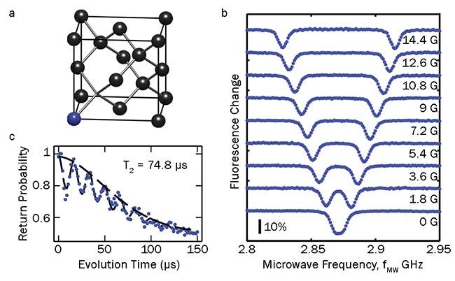
Figure 1. The basics of nitrogen-vacancy (NV) center spins in diamond. The crystal structure of the NV
center (a). Optically detected electron spin resonance, which forms the basis for most magnetometry
applications (b). Spin coherence decay measurements (c). The typically long NV spin coherence times
can be exploited to further enhance magnetic-field sensitivities of NVs. Courtesy of University of Basel.
Magnetometry based on NV center spins measures the energy shifts — or, equivalently, shifts in the quantum-
mechanical phase — that a spin experiences in the presence of a magnetic field. The ODMR traces shown in Figure 1b represent the simplest method of implementation of such single-spin magnetometry, where the splitting between the observed ODMR resonances is directly proportional to the magnetic field that the NV spin experiences.
For spin-based magnetometers, the magnetic field sensitivity η scales with
1/T21/2, where T2 is the characteristic time-scale over which the quantum nature (i.e., the coherence) is preserved. In the case of ODMR-based magnetometry, T2 is ultimately connected to the observed ODMR linewidth; for typical values T2 * ~1 μs yields η ~1 μT/Hz1/2.
However, coherent control of spins permits the extension of coherence times. Figure 1c shows a typical case, where a spin coherence time T2 = 74.8 μs is achieved using a Hahn echo sequence.
More advanced techniques have expanded T2 to tens of milliseconds, which can improve sensitivity by up to two orders of magnitude2.
To exploit these attractive properties for nanoscale quantum sensing, the NV sensor needs to be brought in close proximity to a sensing target, ideally to within just a few nanometers. The most flexible approach applies a scanning probe geometry, which scans the NV and sample with respect to each other for imaging. Today, the most robust and sensitive implementation of such scanning NV magnetometry is achieved by using diamond nanopillars that contain individual NV centers at their tips as scanning probes (Figures 2 and 3). This approach, originally conceived in 20123, has since been refined4 to the extent that commercial solutions are available today from companies such as Swiss startup Qnami AG.
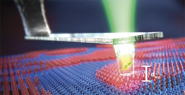
Figure 2. An artist’s rendering of an all-diamond tip containing a single-electron spin quantum sensor at its apex. The spin scans at a distance of dNV ~20 nm over a sample surface, where dNV defines the ultimate imaging resolution of the approach. Courtesy of University of Basel.
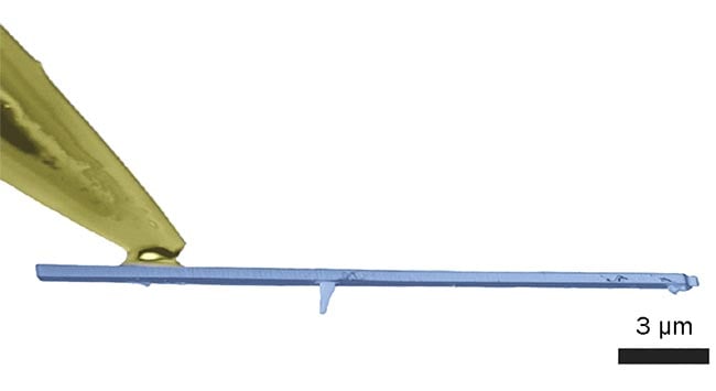
Figure 3. A scanning electron microscopy image of a nanoscale quantum sensor fabricated from a high-purity, single-crystal diamond. Courtesy of University of Basel.
These diamond tips enable detection of
single-electron spins by stray-field imaging at resolutions around 20 nm. Further,
the technique operates under ambient conditions and in cryogenic environments5. These combined properties render scanning NV magnetometry a highly promising tool for nanoscience — and
nanotechnology, in general — and for the
study of electronic phenomena in the solid
state in particular.
To date, demonstrations of a variety of NV magnetometry applications have gone beyond the proof-of-concept stage, and they have revealed new scientific findings that would have been impossible to achieve otherwise. These include quantitative imaging of magnetic domains and domain walls, magnetic imaging of atomically thin ferromagnets5, nanoscale electronic transport studies6, the determination of spin chemical potentials in ferromagnets7, and, most surprisingly, the imaging of spin textures in antiferromagnets8. Multiferroics and antiferromagnets are expected to
be key contenders for next-generation electronic devices.
These and other examples rely strongly on robust implementation of new sensing modalities of NV magnetometry. In addition to dynamical decoupling, another notable example is spin relaxometry, where the environment’s influence on NV spin relaxation rates is exploited as a sensing resource. These interesting approaches primarily target sensitive detection and imaging of fluctuations of alternating current (AC) magnetic fields from the megahertz to the gigahertz range. This can be applied to microwave current imaging, for example, and other characterizations of electronics.
New approach to quantum sensing
A typical quantum sensing experiment starts by initializing the NV center’s electron spin with a laser pulse lasting a few microseconds, follows with a microwave pulse sequence that encodes the sensing protocol, and finishes with the readout of the electron spin by a second laser pulse and simultaneous detection of redshifted fluorescence photons (Figure 4).
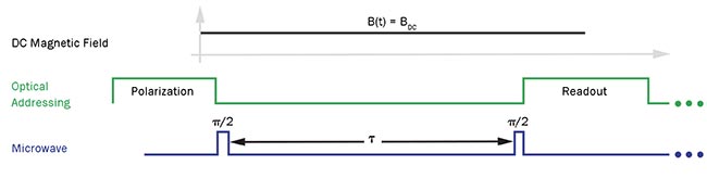
Figure 4. Typical NV magnetometry sequences using a Ramsey pulse sequence on the NV spin. Optical excitation is used to initialize and measure the NV spin. Courtesy of University of Basel.
This approach requires strong microwave fields at the NV center position, which are achieved most efficiently by placing a thin wire in the center’s vicinity. Control of the electron spin is implemented with a microwave synthesizer
that is switched on and off via a high-isolation switch. Isolation well above
60 dB is crucial to avoid affecting the
electron spin when it is performing its sensing function between control pulses. The rise and fall times of the switches should last no more than a few nanoseconds — a limit imposed by the typically achievable Rabi frequencies for the atomic transition, which can reach several tens of megahertz.
A multichannel digital pattern generator can control both the laser and microwave switches. The fidelity of the microwave pulses is determined by the accuracy of control over pulse length, which requires a digital pattern generator able to deliver a timing resolution of about 1 ns.
Traditionally, pulse sequences were described as bit strings, where one bit is consumed per sample clock tick. This approach requires a large sample memory and results in long instrument upload times. More recent methods use run length encoding to describe pulse sequences, wherein each pulse is described by an integer number that encodes its duration in clock ticks. For the sparse pulse sequences typical in quantum sensing protocols, this encoding improves upload time and greatly facilitates instrument programming.
A typical quantum sensing experiment repeats the measurement sequence many times and the accumulated photon count encodes the probability of the spin state of the final measurement. More advanced protocols have demonstrated that single-shot detection of the electron spin state9 can reduce the measurement time. Yet, for most practical quantum sensing applications, multishot spin readout experiments remain the preferred choice10. In either case, the spin readout is facilitated by versatile processing of the single-photon detection events.
Most quantum sensing experiments proceed with a parameter sweep of the interrogation time, which is often equivalent to the interpulse spacing in the sensing sequence. In such cases, one sensing measurement consists of a set of pulse sequences. Cycling through all pulse sequences mitigates optical and thermal drifts. Exploiting two triggers can help achieve this — the trigger that marks the start of a laser pulse and the trigger that marks the sequence number. Using these triggers enables binning of detected fluorescence photons into a two-dimensional histogram that encodes the temporal
fluorescence response of the readout laser pulse for each sensing sequence. This represents a multidimensional time-
correlated single-photon counting experiment.
Traditionally, such experiments have been performed with hardware correlators. More recently, companies such as Swabian Instruments have applied modern single-photon counting approaches to enable fast on-the-fly processing of single-photon detection events in a flexible fashion. Such approaches eliminate common hardware limitations, such as limited histogram range and bin numbers, and greatly facilitate the implementation of novel quantum sensing methods.
Current hardware developments in quantum sensing aim for exquisite degrees
of control, calling for pulse pattern generation and arbitrary waveform generation with a timing resolution below 100 ps.
At the same time, with the availability of fast and low-deadtime superconducting nanowire single-photon detectors, fast high-throughput electronics are needed to process single-photon events at rates beyond 100 MHz, with timing resolutions in the few-picosecond range. The development of such electronics and processing systems are challenges that call for innovative solutions.
Compact, fast modulated lasers
Initializing the spin state of NV centers and reading it out after the microwave manipulation, as shown in Figure 4, requires precisely tailored light pulses. Specifically, pulses should exhibit the following parameters:
• An emission wavelength within the excitation spectrum of NV− centers between 510 and 560 nm.
• Fast modulation with rise and fall times under 10 ns.
• An on/off extinction ratio over 60 dB.
• A good Gaussian beam profile.
• High spectral purity.
Some quantum sensing applications also require the ability to generate pulse trains with arbitrary on/off times and excellent intensity stability.
Until recently, the most common approach to generating such laser pulses involved the combination of a 532-nm continuous-wave laser with a double-path acousto-optical modulator (AOM). However, these laser-AOM setups are difficult to align, they are bulky, expensive, and sensitive to shocks, and they require a large or active heat sink. Since 2018, laser diodes at 515 nm with direct intensity modulation have offered an alternative solution for use in lab setups and commercial systems.
The main advantages of these laser
diodes are their modulation capabilities, such as fast analogue and digital modulation with true off state, as well as precise real-time intensity control without the need for an external modulator. They also enable integration of electronics, optics, and a single-mode fiber coupling into a compact and rugged platform. This allows user-friendly integration with quantum sensing setups, longer lifetimes without the need for alignment or maintenance, and a more compact footprint.
Laser diodes enable live control of the output power via transistor-transistor logic (TTL) input with rise and fall times below 2.5 ns and on/off extinction ratios
above 70 dB. Figure 5 shows typical modulation characteristics of a 515-nm laser diode with a modulation frequency of
10 kHz. The lasers can withstand shocks up to 60 G, as well as high and low temperatures when built with rugged manufacturing technologies, such as HTCure from HÜBNER Photonics. This makes them suitable for use in harsh environments.
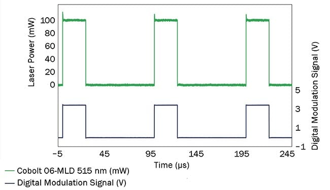
Figure 5. Output power trace over time of a recently released modulated 515-nm laser diode. The modulation characteristics of the 2020 model were optimized for quantum applications. Dual modulation: 10 kHz, 25% duty cycle. Courtesy of HÜBNER Photonics.
As high-purity diamond quantum
sensing cantilevers emerge alongside dedicated control and measurement electronics and high-quality laser sources, the tools for versatile scanning probe quan-
tum sensing experiments are increasingly accessible to a broader audience. Enterprises around the world have also started integrating NV-based ensemble quantum sensors into commercial chip packages, with the goal of realizing the first mass-produced products that leverage quantum-enhanced sensing. Further breakthroughs promise to transform quantum sensing technologies into a versatile range of sensor products.
Meet the authors
Niklas Waasem is regional sales manager and application specialist for HÜBNER Photonics.
He completed a doctorate in physics at the Fraunhofer Institute for Physical Measurement Techniques (IPM) in cooperation with the
University of Freiburg; email: [email protected].
Helmut Fedder is CEO and co-founder of Swabian Instruments. He studied physics in Germany, Sweden, and the Netherlands and has more than eight years of experience as a research group leader in quantum optics, FPGA development, and experiment design; email: [email protected].
Patrick Maletinsky is a professor at the
University of Basel and the leader of its quantum sensing group, which he established in 2012. He obtained a doctorate from ETH Zürich before moving to Harvard University, where he contributed to the early developments of quantum sensing; email: [email protected]
References
1. M. Chernobrod et al. (2005). Spin microscope based on optically detected magnetic resonance. J Appl Phys, Vol. 97, Issue 1,
p. 014903.
2. N. Bar-Gill et al. (2013). Solid-state electronic spin coherence time approaching one second. Nat Commun, Vol. 4, article 1743.
3. P. Maletinsky et al. (2012). A robust scanning diamond sensor for nanoscale imaging with single nitrogen-vacancy centres.
Nat Nanotechnol, Vol. 7, p. 320.
4. N. Hedrich et al. (2020). Parabolic diamond scanning probes for single spin magnetic field imaging, www.arxiv.org/abs/2003.01733v1.
5. L. Thiel et al. (2019). Probing magnetism
in 2D materials at the nanoscale with single-spin microscopy. Science, Vol. 364, p. 973.
6. S. Kolkowitz et al. (2015). Probing Johnson noise and ballistic transport in normal
metals with a single-spin qubit. Science, Vol. 347, p. 1129.
7. C. Du et al. (2017). Control and local
measurement of the spin chemical potential in a magnetic insulator. Science, Vol. 357, p. 195.
8. P. Appel et al. (2019). Nanomagnetism of magnetoelectric granular thin-film antiferromagnets. Nano Lett, Vol. 19, p. 1682.
9. B.J. Shields et al. (2015). Efficient readout
of a single spin state in diamond via spin-
to-charge conversion. Phys Rev Lett,
Vol. 114, p. 136402.
10. J.F. Barry et al. (2020). Sensitivity optimization for NV-diamond magnetometry.
Rev Mod Phys, Vol. 92, p. 015004.