HAIFA, Israel, April 19, 2021 — Researchers from Technion-Israel Institute of Technology demonstrated an approach for obtaining images of evanescent waves that uses nonlinear wave-mixing. The microscopy method allowed the researchers to fully reconstruct the electromagnetic field of the evanescent waves and to perform real-time monitoring of wave-pattern changes.
Nonlinear wave-mixing combines two or more light beams, including one that is very intense, to generate a new electromagnetic wave of a different color; the phenomenon commonly occurs in semiconductors, dielectrics, and metals. The Technion researchers mixed a wide and intense pulsed light beam with evanescent waves moving across the surface, generating a new lightwave that could be subsequently detected by regular means.
Evanescent waves are a byproduct of photonic integrated circuitry, which uses guided lightwaves in a manner analogous to electronic circuitry. The guided waves do not radiate outside of their host structure, but they do leave a fast-decaying signature in the air. That feature is known as an evanescent wave.
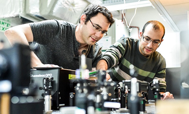
Kobi Frischwasser, left, and Kobi Cohen of the Advanced Photonics Research Lab at Technion. Courtesy of Technion-Israel Institute of Technology.
Because their energy remains bound to the surface, evanescent waves cannot be detected with standard microscopy methods. Specialty methods can detect these waves either by using a small needle approaching the surface and scattering out the electromagnetic power in its vicinity or by firing electrons on the surface and characterizing their subsequent spectra.
Though these two techniques are able to provide a high spatial resolution, they rely on complex and designated infrastructure. They also have long acquisition times that prohibit real-time guided waves.
The idea to overcome that challenge, said Kobi Frischwasser, lead author of a paper describing the new approach, emerged when the author was exploring nonlinear methods for coupling light into confined optical modes.
“I realized that it could also work the other way around — the information in such modes can be coupled nonlinearly out,” Frischwasser said. “I never imagined that this new microscopy scheme could open up new and, so far, unattainable opportunities for near-field science.”
“Aside from bulk materials, nonlinear wave-mixing naturally takes place at any interface between two materials, making it an ideal platform for nanophotonics — which often deals with light at interfaces,” said Guy Bartal, leader of the project and a professor of the Andrew and Erna Viterbi Faculty of Electrical Engineering. “Below some spatial limit, information remains bound to the surface and cannot be seen by any camera. Our technique ‘releases’ this information into radiation that can be detected — even with a commercial camera!”
The method, nonlinear near-field optical microscopy (NNOM), requires only a powerful commercial laser source and standard optical components and detectors.
In testing the method, the researchers found that they were able to extract a surprising amount of information. “By changing the polarization of the high-intensity pulses, we could see different shapes,” Bartal said. “We then found out that we are not just measuring the evanescent waves, but we can choose what information to take out of them.”
The team successfully separated and visualized the information stored on the “spin” of the evanescent waves, that is, the clockwise and counter-clockwise rotation of the electric field on the interface.
“When you process the optical information in free-space, everything is much easier,” said team member Kobi Cohen. “We could see the spatial frequency content of the surface waves, not just the real-space shape, and through a reconstruction algorithm, we managed to extract their phase as well. From here on out, the road to a full-field reconstruction was clear.”
The authors demonstrated the application of NNOM by monitoring the changes in digitally encoded surface waves via the use of a spatial light modulator.
“We wanted to show that this new microscopy scheme can have practical applications,” Shai Tsesses said. “Since there are times when you need to make sure of the exact evanescent pattern, such as in optical trapping and manipulation experiments or when trying to optically address quantum emitters in nanophotonic platforms.”
“We haven’t even begun to explore the limits of this scheme and its applications,” Frischwasser said. “It may very well help us to develop better methods of verification for photonic circuitry. We are very excited about the future and hope that many groups around the world will join us in our quest.”
The research was published in Nature Photonics (www.doi.org/10.1038/s41566-021-00782-2).