Imaging technologies that reveal the world beyond our visual range are helping to enhance public health, food quality, and product inspections.
HANK HOGAN, CONTRIBUTING EDITOR
The ability to image beyond the visible spectrum offers more than a quantitative expansion of our perceptions. It also provides qualitative improvements with applicable value to public health, manufacturing, and the safety and quality of food. These and other applications are benefiting today from advancements in higher sensor resolutions, new lighting strategies, and more cost-effective system-level designs.
Nonvisible imaging covers technologies operating outside the visible spectrum, which extends from roughly 380 to 750 nm. Below 380 nm, this imaging involves modified conventional silicon sensors with UV-appropriate optics, filters, and lighting. Above 750 nm, the range of infrared sensors, lens materials, light sources, and imaging modalities is much broader.
Thermal imaging heats up
Thermal cameras targeting the longwave infrared (LWIR), for example, gather image data differently than most other devices. Rather than capturing light reflecting off an object, they detect photons emitted by the object itself.
Imaging in the LWIR, which runs from about 5 to 15 µm, recently received a boost from the COVID-19 pandemic due to the ability of LWIR sensors to measure variations in skin surface temperature at a distance.
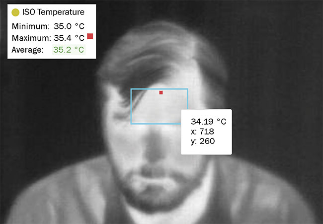
Thermal imaging has received a boost during the COVID-19 pandemic, due to the technology’s potential value in supporting remote health screening. Courtesy of Nuvoola AI.
Camera systems for this application generally focus on areas around the eyes’ tear ducts, which correlate most closely to body temperature according to best practices outlined by IEC 80601-2-59:2017 and ISO/TR 13154:2017 standards. Accurately screening subjects for fever requires thermal cameras capable of capturing several frames of data with a 20- × 20-pixel array, assuming the subject’s face is in close proximity to
the device.
“To be able to measure somebody at 6 ft away, you need a high-resolution camera,” said Jean-Marc Taillon, vice president of operations and strategic growth at Nuvoola AI, a Montreal-based software firm.
The company recently announced a kiosk that leverages imaging to help limit the spread of the COVID-19 virus at the workplace and elsewhere. The system incorporates a visible camera, a LWIR microbolometer, and a blackbody source. After a user answers health screening questions at the kiosk, Nuvoola AI’s system checks the orientation of their face and determines if they’re wearing a mask before the LWIR camera captures a series of thermal measurements. The blackbody source is at a known temperature and is in the frame of the thermal camera, ensuring measurement accuracy.
For this application, Nuvoola AI partnered with Teledyne DALSA, which
supplied an uncooled microbolometer camera with a video graphics array (VGA)-resolution 640 × 480 array of 17-µm pixels. The camera has an accuracy of ±1 °C at room temperature and a thermal contrast — the ability to spot small temperature differences — of ≤50 mK.
Jean Brunelle, product manager for LWIR camera and sensor products at Teledyne DALSA, said super-extended graphics array (SXGA)-resolution cameras with array sizes of 1280 × 1024 pixels are available, but he noted that these are not cost-effective solutions for most applications. To get to higher pixel densities, the industry has been transitioning from 17-µm pixels to 12-µm pixels over the last few years.
“Our VGA 12-µm pixel platform is currently in the final stages of development and will be a steppingstone to bring us SXGA resolution in the coming years,” Brunelle reported.
One way to get around current LWIR resolution limitations is to use a combination of LWIR and visible cameras, said Markus Tarin, president and CEO of MoviTHERM of Irvine, Calif. The data streams from a thermal sensor, and a multimegapixel visible sensor can create a composite that provides apparent heat image data with higher resolutions than what is achievable with thermal cameras alone.
Tarin used this approach when solving the problem of how to take temperatures remotely in a health screening application. He leveraged AI software to locate the subject’s eyes in a visible camera image before the thermal camera captured the temperature of the area near the eye.
Currently, thermal cameras that offer megapixel or higher native resolution are expensive. Less costly versions could pay dividends in temperature screening applications, as well as for tasks such as inspecting packages to ensure they have been properly heat sealed.
Such applications might require inspecting the temperature distributions of a strip measuring 0.2-in. wide from a distance of 40 in. as the package travels down a conveyor belt. This is a feat difficult to pull off without a thermal camera offering megapixel or higher resolution, and such cameras must be cost-effective.
According to Tarin, uncooled microbolometers, the most common thermal imaging technology, cost as much as $50,000 two decades ago. The price for these sensors has fallen by a factor of 10 or more since then, leading to wider adoption of the technology. Tarin expects cost reductions to continue.
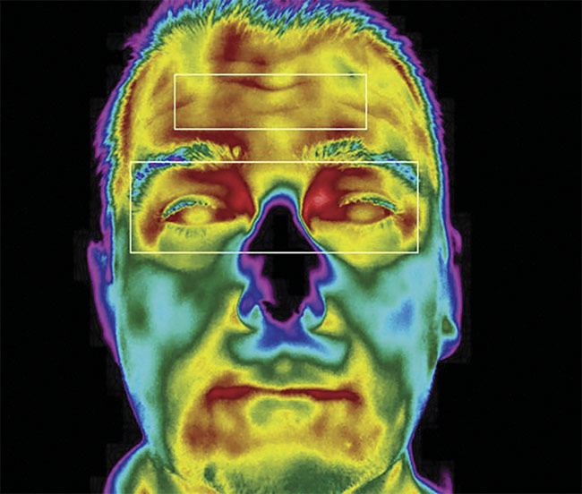
The inner canthi (i.e., the tear ducts) are the parts of the human face that correlate most closely to body temperature, and thermal camera systems designed for health screening applications should cover this area of the face with a minimum of 3 × 3 pixels, and ideally more. Courtesy of MoviTHERM.
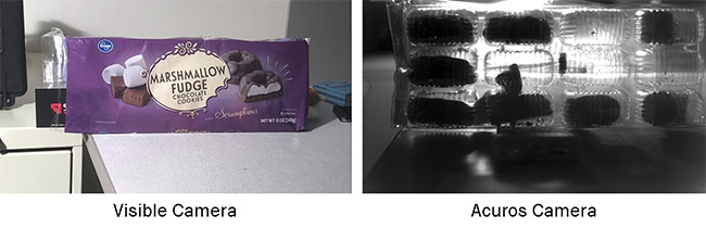
Shortwave IR (SWIR) cameras can capture image data of the internal contents inside otherwise opaque packaging. Courtesy of SWIR Vision Systems.
Sensors aside, other thermal imaging components still come at a higher price than is the case for their visible imaging counterparts. “The lens material in the mid- and long-[infrared] range is typically germanium,” Tarin said. “It’s an exotic semiconductor material. So, the lenses are very expensive.”
Long on shortwave IR
Applications are also growing in the shortwave infrared (SWIR) range, which extends from 0.9 µm to about 1.7 µm. Sensors based on indium gallium arsenide (InGaAs) are the prevailing commercial technology, though quantum dot sensors are attempting to make inroads. Both camera technologies are seeing increased interest due to the imaging capabilities offered.
Tarin noted, for instance, that while a dropped piece of fruit may be damaged, bruising may not be visible to the eye for days. A SWIR camera, however, would reveal the damage much sooner. SWIR imagers — as well as those operating
in the midwave IR (MWIR) from 3 to
5 µm — can also help measure the sugar content of fruits and other foods because of chemical bonds that absorb in those parts of the spectrum.
Many plastics that are opaque in the visible are transparent to SWIR light, while dyes commonly used in products such as detergents have strong absorption bands in that spectrum. Such differences make inspecting the fill levels of detergent bottles possible using SWIR imaging. Teledyne DALSA’s line of SWIR cameras employ the most widespread imaging technology: InGaAs hybridized onto a CMOS circuit. Although these detectors and cameras can cost several times more than their CMOS counterparts, Teledyne DALSA and other suppliers are working to make the technology more accessible and affordable. Currently, commercial SWIR sensor pixel sizes run about 10 µm, and arrays about 1 MP.
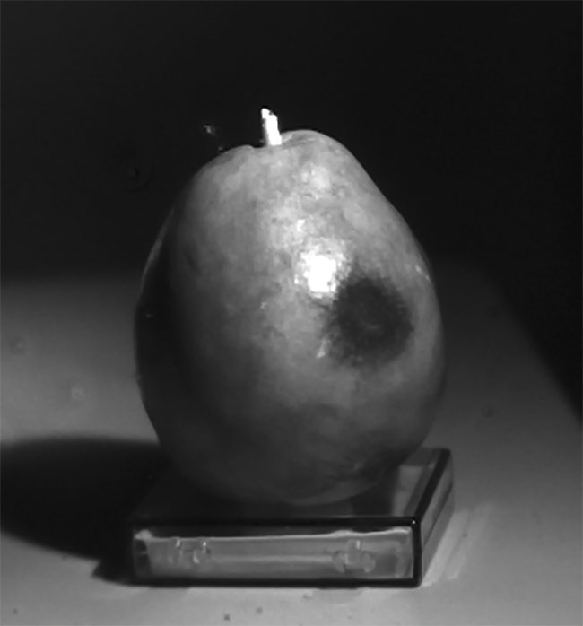
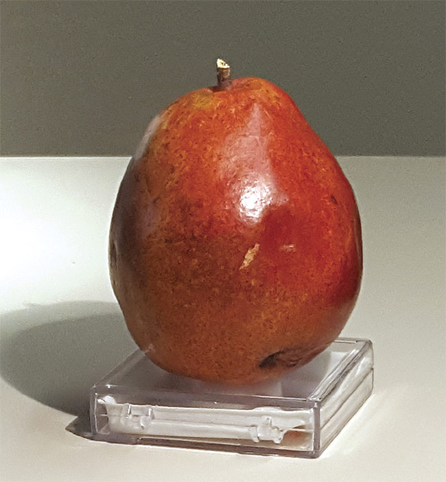
Water’s strong absorption peak in the SWIR range clearly discloses bruising on fruit (top) that is not as evident in the visible range (bottom). Courtesy of SWIR Vision Systems.
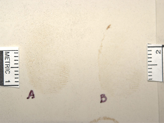
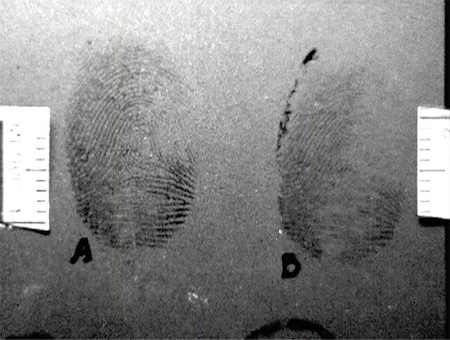
Latent fingerprints appear faintly to cameras capturing visible light (top), but are much more evident at UV wavelengths (bottom), even without processing. Courtesy of Oculus Photonics.
Other new developments include higher
resolutions via smaller pixel sizes along with greater spectral coverage. In May 2020, Sony announced an image sensor with 5-µm pixels and megapixel resolution. Due to an innovative connection technology on the bottom of the SWIR-sensitive InGaAs layer, the sensor has a topside indium phosphide layer responsive to visible light that can be made thinner than otherwise possible. As a result, the sensor images from 0.4 to 1.7 µm,
spanning the visible, near-IR, and SWIR spectra.
Sensors based on quantum dot technology are also expanding the spectral range of SWIR cameras, according to George Wildeman, CEO of SWIR Vision Systems. The Durham, N.C.-based startup has commercialized imagers that layer quantum dot films directly onto CMOS wafers, with the quantum dot structures fabricated to sense specific wavelengths of interest.
The company has commercialized a 2.1-MP SWIR camera and demonstrated sensors with pixel pitches <3 µm in the lab, Wildeman said, adding, “The inherent scalability of this technology makes future low-cost and very high-resolution sensors possible for very high-volume applications such as mobile electronics and automotive sensing.”
The technology’s quantum efficiency is currently only 20%, much lower than the 70% conversion of InGaAs sensors. However, in many industrial imaging applications, additional IR and SWIR photons can be provided by bright, low-cost light sources, Wildeman said.
He added that quantum dot sensors can also enable a single sensor to capture wavelengths spanning the visible range all the way out to 2 µm. “We believe broader imaging bandwidths will be critical for many applications,” Wildeman said. The region from 1.7 to 2 µm offers particular interest for applications in chemical sensing, plastic recycling, silicon inspection, and laser beam profiling.
Going short: UV imaging
Imaging technology also peers below the visible to acquire data from the UV spectrum. Standard silicon sensors can capture longwave UV light centered around 360 nm, provided the cover glass and on-pixel microlenses are not coated with UV-blocking films, said Austin Richards, a principal at Oculus Photonics, which designs, manufactures, and sells UV imaging systems.
Imaging from 200 to 300 nm, however, requires more exotic technology. Such systems still use a silicon sensor, Richards said, adding, “But the silicon is back-thinned and backside-illuminated, and there are no microlenses on it.”
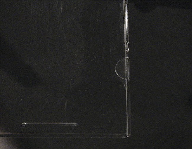
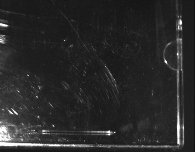
Faint scratches on glass and plastic are often much more apparent when imaged under UV light. This is evident in these two images of a CD jewel case captured with a visible-range sensor (top) and a UV camera (bottom). Courtesy of Oculus Photonics.
Many materials transparent in the visible appear opaque in the UV, which makes it easier to image defects such as minute scratches on glass and other ma-
terials. UV imaging can also pick up latent fingerprints on surfaces without the need for dusting or other processing. This can be a boon to forensics, Richards said.
One of the key challenges to UV imaging is achieving adequate light levels. There are generally far fewer ambient UV photons to work with than is the case when imaging in the visible range. UV cameras can compensate for this by employing pixels measuring 5 µm versus the 1-µm pixels applied by visible sensors. Another workaround is illumination from artificial light sources, such as LEDs at longwave UV, or fluorescent bulbs at shortwave UV. These sources may provide sufficient intensity if bright enough and properly focused.
As component and system-level advancements continue to improve the capabilities and costs of nonvisible imagers, the sector is on track to deliver some very visible future gains.