
Novel Integration Helps Solve Imaging Bottleneck
Engineers at imec have integrated a pinned photodiode (PPD) structure in thin-film image sensors. According to the researchers, the addition of a pinned-photogate and a transfer gate into the thin-film image sensor architecture exploits the superior absorption qualities of thin-film imagers — beyond 1 µm.
Further, they said, the integration shows show that thin-film-based image sensors with a pinned photodiode structure can exhibit noise performance that is comparable to a silicon pinned photodiode pixel.
As a result, the advancement unlocks the potential of sensing light beyond the visible in a cost-efficient way.
Though the use of III-V materials can overcome this long-held detection range limitation, the manufacture of these absorbers is expensive, which limits their use. In contrast, sensors using thin-film absorbers such as quantum dots have recently emerged as a promising alternative; they have superior absorption characteristics and hold potential for integration with CMOS readout circuits. Nonetheless, such infrared sensors have an inferior noise performance, which leads to poorer image quality.
The PPD structure was introduced for silicon-CMOS image sensors over 30 years ago. This structure introduces an additional transistor gate and a special photodetector structure, by which the charges can be completely drained before integration begins. In turn, these qualities allow the user to reset operation with neither thermal noise nor the effect of the previous frame.
Because of lower noise and improved power performance, PPDs dominate the consumer market for silicon-based image sensors.
However, beyond silicon imaging, incorporating this structure was not possible up until now because of the difficulty of hybridizing two different semiconductor systems.
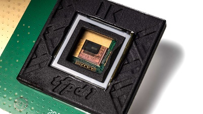
Imec researchers integrated a pinned photodiode structure in thin-film image sensors. The development charts a course for cost-efficient visible light sensing with favorable detection capabilities and manufacturability. Courtesy of imec.
The imec researchers monolithically hybridized a shortwave infrared (SWIR) colloidal quantum dot photodetector with an indium-gallium-zinc oxide (IGZO)-based thin-film transistor into a PPD pixel. This array was subsequently processed on a CMOS readout circuit to form a superior thin-film SWIR image sensor.
According to imec project leader Nikolas Papadopoulos, the prototype 4T image sensor based on the organic absorber showed a remarkable low read-out noise of 6.1e−, compared to >100e− for the conventional 3T sensor. As a result, infrared images can be captured with less noise, distortion, or interference, and with greater accuracy and detail. The researchers also reported a quantum efficiency of 54% at 940 nm.
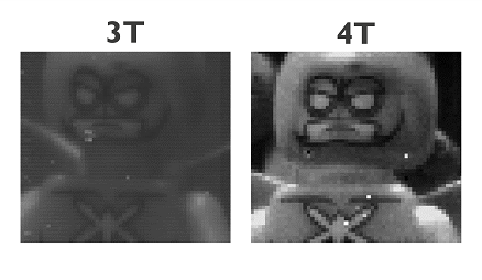
The image portrays a comparison in quality between the conventional 3T image sensor and the imec researchers' 4T pixel image sensor. The imec group monolithically hybridized a SWIR quantum dot photodetector with an indium-gallium-zinc oxide (IGZO)-based thin-film transistor into a PPD pixel. The researchers then processed the array on a CMOS readout circuit. Courtesy of imec.
The researchers said that future steps for the integration include broadening the application of the sensors beyond those used for silicon imaging.
The research was published in Nature Electronics (www.doi.org/10.1038/s41928-023-01016-9).
/Buyers_Guide/Imec/c22187