To increase the use of thermal imaging, a technology that provides a good image and is low-cost, easily scalable and low in power is required.
Daniel Ostrower, RedShift Systems Inc.
The desire to “see” in complete darkness or through obscurants such as smoke or fog has driven the development and adoption of thermal imaging technology in numerous industries. Thermal imaging translates a scene’s heat signature — the long-wavelength infrared energy produced in the 8- to 14-μm waveband — into digital data that can be used to produce a visible image or be fed into a computer for interpretation.
Because the thermal energy of a scene is independent of reflected light and because it can travel through obscurants with small particle sizes, thermal imaging is the technology of choice for imaging in the dark or in other difficult environmental conditions.
Despite the reduced cost of thermal imaging available with today’s uncooled sensors, the technology is still unattainable for millions of potential users. A typical uncooled camera may cost in excess of $10,000 — too much for most potential customers.
For example, thermal imaging is critical for firefighters because it helps them locate downed victims, pinpoint the source of a burn or escape a building that is in a dangerous condition, but because of the high price, only a small fraction of firefighters use thermal imaging cameras regularly. To be universally applied to firefighting and other applications, the technology must be inexpensive, easily scalable and low in power and must provide a good image quality.
Today’s technology
The most common form of thermal imaging technology available today is the microbolometer sensor. Although microbolometers have greatly reduced the price of thermal imaging (compared with older “cooled” technology), microbolometer-based cameras still range from $8000 to $20,000, depending on resolution, performance and features. In addition, they are manufactured in dedicated foundries, which makes them expensive to produce, and they require a highly complex multimask step design.
Expensive die-level packaging is necessary because microbolometers cannot be exposed to the high temperatures used for inexpensive wafer-scale packaging. They are not easily scalable: The cycle time for new microbolometer designs takes several years and costs millions of dollars. Microbolometers also are limited in their power consumption, needing ~2 W for normal operations — and even higher for larger array sizes. The image quality is somewhat limited, too. Large-pixel microbolometer designs have demonstrated enough sensitivity for current applications, but performance in smaller-pixel future applications may be limited.
A new technology with significant changes in underlying design, materials and manufacturing processes is required to make universal deployment of thermal imaging a reality. Optical thermal imaging can accomplish that.
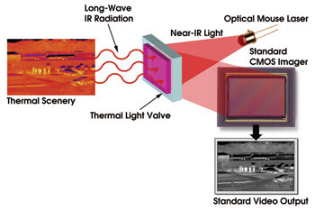
Figure 1. The Thermal Light Valve is the part of the optical thermal imaging system that shifts long-wavelength IR to CMOS-visible IR wavelengths.
Optical thermal imaging technologies rely on temperature-dependent changes in optical properties to produce thermal images. Such changes are optically, rather than electrically, read out using standard digital camera electronics.
A chip known as a Thermal Light Valve shifts long-wavelength IR to CMOS-visible IR wavelengths (Figure 1). The chip is composed of narrow-band optical filter pixels standing on thermally resistive posts on an optically reflective and thermally conductive substrate (Figure 2).
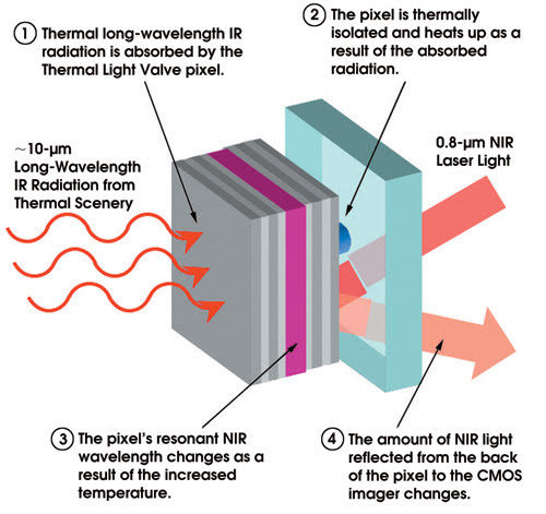
Figure 2. The chip is made of narrowband optical filter pixels.
Each pixel of the chip acts as a passive wavelength converter. Long-wavelength infrared radiation from the scene is imaged onto and absorbed by the Thermal Light Valve. Thermal pixels on the array then heat up in a way that is directly related to the thermal signature of the scene.
The minimum reflective wavelengths of the pixels shift based upon the thermal energy incident on each. A narrowband near-infrared light source is used to “probe” the temperature of the pixels across the chip. This probe signal is reflected off the chip — in amounts that depend on the pixel temperature — and onto the CMOS imager (Figure 3). The intensity of the light received by the CMOS imager is therefore “modulated” by the heat signature of the scene.
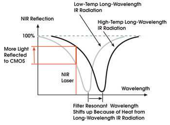
Figure 3. An NIR probe signal is reflected off the chip in varying amounts — depending on the pixel temperature — and onto the CMOS imager.
A thermal image is obtained by using CMOS imagers to measure the pixel-to-pixel variation in reflection of the NIR probe signal.
Tunable filter
The device’s tunable optical filter is a Fabry-Perot structure made from amorphous silicon (a-Si) and silicon nitride (SiNx) thin films, which have been used extensively for many years in solar cells and in flat panel displays. These materials are deposited using plasma-enhanced chemical vapor deposition, which can produce uniform, dense materials in high-volume-manufacturing environments.
The optical filter’s minimum reflective wavelength depends on the optical thickness of the cavity — a product of both physical thickness and the index of refraction. Tunability is achieved by changing the index of refraction. The materials are characterized by a high thermo-optic coefficient, which is defined as the change of index of refraction per degree of temperature change.
The manufacturing and packaging are simplified because the sensing array is a passive layer of optical thin films on glass and not an electronic device. It can thus be manufactured in a standard microelectromechanical foundry, taking advantage of foundry economies of scale to dramatically reduce production cost over that obtainable with custom fabrication lines.
The readout circuit in the thermal imaging system consists of off-the-shelf parts, such as laser diodes and CMOS sensors that can be sourced from high-volume optical mouse and consumer camera applications and managed independently from the sensor array. This reduces cost, increases yield and reduces development cycle time because the circuit is not physically coupled to the sensing array and isn’t a custom design.
Cameras based on this technology will be available for less than $3000 in low volumes and will rapidly decrease in price with time and increasing volume. The chip requires only a few mask steps to produce, which means it is less costly to make and has much higher yields.
Easily scalable
Optical thermal imaging will allow new products to be released on a time scale consistent with consumer products. Because the pixel’s thermal isolation does not also have to be electrically conductive, the design is much simpler than microbolometers and can be easily scaled. A change in sensor component is all that is required for new designs.
Cameras based on the technology will consume considerably less than 1 W. Because the chip is passive, it consumes no power, and the back-end electronics are the same as a digital camera.
The thermo-optic materials used are sensitive to temperature changes, which provides a high potential for good image quality. The percent change in signal for a 1 °C change in temperature is up to 20 times higher than in microbolometers.
Optical thermal imaging provides original equipment manufacturers with a new option for developing low-cost, high-performance thermal imaging products for a variety of applications. It will open up markets that have demonstrated a high demand for thermal imaging but that to date have very low penetration because of the price-to-performance ratio of today’s technologies.
Safety and security
For example, auto manufacturers are beginning to introduce active safety systems that rely on sensors to monitor the car’s environment and to prevent accidents before they occur. Applications include pedestrian detection, night vision, lane-departure warning and driver-occupant monitoring. BMW, Honda and GM have all introduced thermal imaging systems in high-end vehicles, but the technology is too expensive for use in mass market vehicles. The key to further penetration is cost reduction. Market research firm Strategy Analytics predicts shipments of almost 20 million automotive cameras in 2010.
According to JP Freeman Associates, the worldwide market for closed-circuit television cameras was $2.6 billion in 2005. Today, more than one-third of this market involves night-vision applications, but the technologies used in these cameras have numerous drawbacks. Thermal security cameras have several advantages, including the ability to see in complete darkness and to detect people and vehicles easily at great distances. At low enough prices, thermal security cameras will be rapidly adopted for surveillance applications such as monitoring parking lots and perimeters.
Thermal imaging allows users to see in the dark or through obscurants. The several generations of technology that have been developed have been adopted by only a small percentage of potential consumers because of their high costs. Optical thermal imaging-based cameras could deliver the low cost, easy scalability, low power consumption and high image quality to spur universal deployment.
Meet the author
Daniel Ostrower is senior director of product management for RedShift Systems Inc. in Waltham, Mass.; e-mail: [email protected].