As demand for data bandwidth grows, co-packaged and on-board optics aim to reduce power consumption per bit while achieving higher channel densities.
NIKOLAUS FLÖRY, VARIO-OPTICS AG
Co-packaged optics (CPO) and on-board optics (OBO) are not novel concepts, per se. The benefits of moving optics closer to the computing cores of data center switches have been clear to systems developers since optical glass fiber was first adopted for long-haul optical transmission. But although the task is relatively straightforward to replace electrical wires with glass fibers in long-distance networks, the technological complexity of integrating optics at the board or module level has proved to be more challenging.
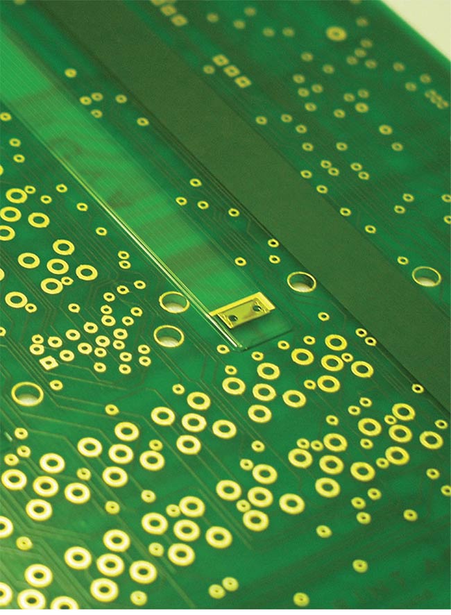
An electro-optical circuit board treats the optical layer as an additional (spacer) layer in the particle circuit board (PCB) design process. The waveguides can be manufactured directly, either by using the PCB as a substrate or in a separate step, before being laminated with the rest of the stack. Courtesy of vario-optics AG.
Nevertheless, the growing demand for higher data throughput at lower power consumption is unlikely to end soon. And because developments in photonic integrated circuit (PIC) transceivers and embedded waveguide systems continue to pick up speed, attention to OBO solutions has also accelerated tremendously in recent years.
CPO vs. OBO
The main limitations of conventional electronic particle circuit boards (PCBs) for high-speed (high-frequency) data transmission derive from the fact that the insertion loss of copper traces scales with frequency. Thus, both the electrical interconnects and the signal generation itself consume more power as transmission frequencies increase.
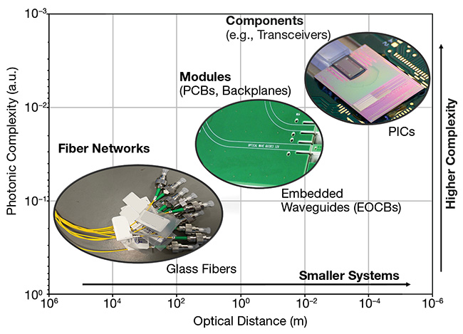
As the photonic building blocks for information and communications technology decrease in size, their complexity increases. These building blocks have only recently begun to achieve the maturity to enable implementation of embedded board-level waveguides and chip-level photonic integrated circuits (PICs) data center hardware. EOCBs: electro-optical circuit boards. Courtesy of vario-optics AG.
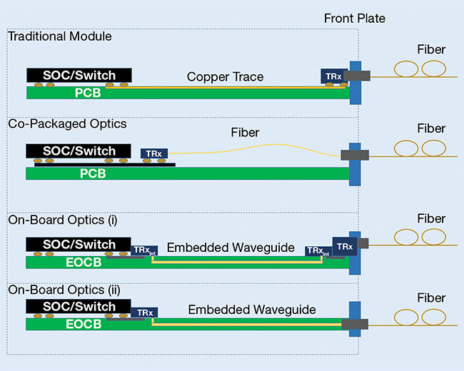
A comparison of various co-packaged optics (CPO) and on-board optics (OBO) architectures. Compared to a traditional module, in which a fiber is terminated at the rack’s front plate, CPO and OBO concepts aim to bring the optical waveguide inside the rack. In CPO architectures, additional fibers bridge the optical signal directly to the transceiver chip (TRX SOC). In contrast, OBO architectures employ embedded waveguides to route light at the board level, either in a separate network (and possibly at a different wavelength) or through a direct connection to the external fiber network. Courtesy of vario-optics AG.
For a while, this drawback of electrical interconnects was circumvented in transceiver applications by making use of various types of parallelism — for example, by increasing the number of channels
or implementing different multiplexing techniques — instead of increasing the pure signal rate of a line. However, subsequent generations of transceivers were required to handle 100 Gbit/s or more, which entered a regime in which power consumption became the prime number of interest. As modern data center architectures start to require that more attention be paid to wall-plug efficiencies, this paves the way for the deployment of more power-efficient optical solutions, such as CPO and OBO. Rather than converting optical signals to electrical signals at the module’s front plate, both of these architectures aim to integrate optical components into a transceiver module where they are physically closer to the system-on-a-chip (SOC) computing node, which helps to reduce module power consumption.
The concept of CPO is analogous to adding another fiber connection inside the module between the front plate and the SOC. Although this is rather straightforward and can be accomplished using existing technology blocks, such as fibers or connectors, reliance on such conventional approaches introduces the challenge of fiber handling inside a rack. As channel densities increase, handling and assembly of such modules is not the only problem. It also raises thermal and mechanical considerations because bundles of fibers require space in the rack and also prevent efficient air cooling.
OBO, conversely, represents a different evolutionary step by replacing the additional fibers used in CPO with embedded waveguide interconnects. These waveguides can be integrated into the PCB itself, thereby adding only one more layer to the total thickness of the PCB rather than additional fibers inside the module.
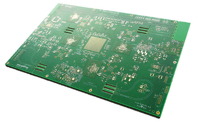
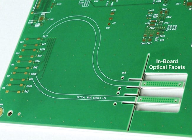
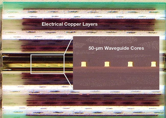
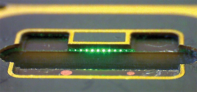
An electro-optical circuit board for an OBO system (top), manufactured by vario-optics, comprises a complex 20-layer electrical stack-up (middle) that incorporates a 50-µm optical multimode waveguide layer (bottom). The optical layer is well protected in the middle of the board and accessed via edge- and in-plane connector interfaces. This design can be equipped with optical engines and a field-programmable gate array to demonstrate multichannel (12×) parallel optical on-board communications. The entire module, including the waveguide layer, can withstand the 270 °C temperatures of standard reflow soldering processes. Courtesy of vario-optics AG.
So far, the most common types of
ma-terials for these embedded waveguides are glass- and polymer-based planar waveguides that can be manufactured in a cost-effective way up to dimensions greater than 20 cm1. Typically, the photonic layer of such an electro-optical circuit board (EOCB) can be manufactured directly on conventional PCB substrates, such as FR4 (flame-retardant epoxy resin) or polyimide. The optical layer is fabricated in a separate step and laminated with the rest of the stack. This allows advanced PCB technologies, such as high-speed radio frequency interfaces
or complex multilayer boards, to be complemented with an optical layer. While there are multiple benefits to this approach, finer points and challenges are associated with the design and manufacture of such EOCBs, however.
Wavelength and mode
Standard long-distance optical telecommunications systems operate at either 1310 nm (the O-band) or at 1550 nm (the C-band). While this presents a logical choice for on-board wavelengths targeting network communications as well, it is
not a necessity, per se. Any transceiver interfacing with fibers outside the rack,
of course, has to be compatible with O- and C-band transmission. Depending on the OBO architecture, however, there is often more flexibility in the wavelengths available for on-board operations.
In many OBO concepts, the optical
circuit is actually separated from the outside circuit and relies on its own media adapters and transceivers, which can be based, for example, on standard VCSELs for on-board communications. This allows the on-board use of other wavelengths, such as 850 nm, which can be more beneficial for the waveguide systems and allow more suitable, cost-effective VCSEL dies.
Similar considerations apply to the choice of single- or multimode waveguides. Any system directly interfacing with the fibers outside the front plate must be compatible with single-mode fibers. Within the board, however, multimode waveguides remain an option that can offer substantial benefits. First, due the larger dimensions of multimode waveguides (for example, a 50-µm core size), they can be fabricated more simply and cost-effectively using different equipment than that used to make single-mode waveguides (for example, a 3-µm core size). This core-size advantage also relaxes the submicron assembly and alignment tolerances characteristic of single-mode assembly to allow relaxed tolerances of several microns, in the case of multimode waveguide production, which further reduces costs.
The flexibility in manufacturing and assembly offsets the cost and complexity associated with the additional on-board transceiver components required when using multimode waveguides on-board.
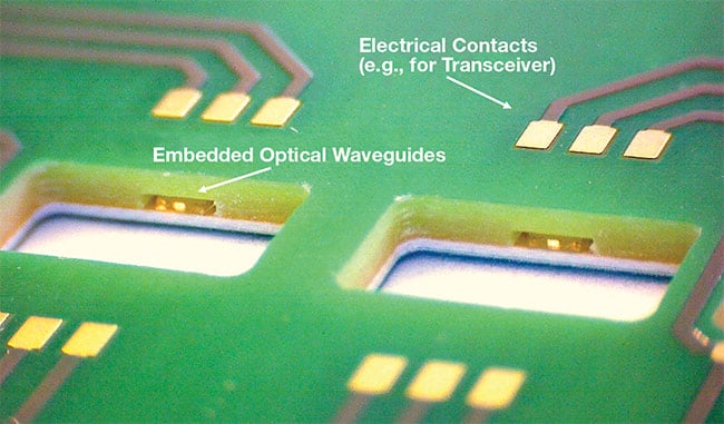
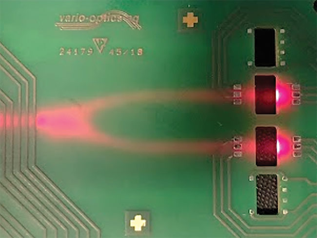
Cavities in an electro-optical circuit board (top) can provide access to the optical layer for in-plane or vertical coupling to transceivers. Splitters and/or combiners (bottom) can be integrated into the photonic circuits for multiplexing and parallel signal transmission. Courtesy of vario-optics AG.
The familiar concerns about limited bandwidth and fading signal quality
arising from modal dispersion can be
neglected as long as the board stays within common PCB dimensions. For
example, multimode waveguide lengths up to 50 cm can achieve open eye
diagrams for transmission rates reaching
250 Gbit/s2. Overall, the options for waveguide core dimension essentially boil down to the choice of board architecture and whether the in-plane waveguides should be directly connected to the fiber network.
Coupling solutions
As the number of transceivers, fiber connections, embedded waveguides, and other photonic components in CPO and OBO systems mounts, the overall impact of the interfaces between them starts to become a fundamental concern. Both in-plane (edge) coupling and out-of-plane (vertical) coupling solutions link embedded waveguides to light sources and
receivers. The coupling schemes of transmitters, however, are heavily influenced by the specific board concept and transceiver components being used.
The use of PICs on CPO platforms that require connections to glass fibers naturally lends itself to in-plane edge coupling. Polymer waveguides are well suited for this purpose. They can be adapted to various mode-field diameters and therefore offer efficient edge coupling to various PIC platforms. Moreover, they can decrease the pitch to below 125 μm, which is a challenge when using traditional fibers3.
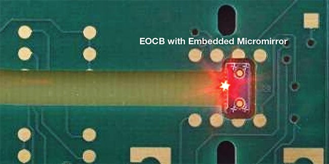
In contrast to in-plane coupling, in which fibers are directly edge-coupled to waveguide facets, vertical coupling requires an element to steer light at a 90° angle. This element can either be integrated into the transceiver chip or placed into a cavity on the board.
Courtesy of vario-optics AG.
Traditional VCSELs, however, are
a good choice for OBO due to their availability and low cost, and they require a 90° deflection into an embedded waveguide. This can be achieved either by adding light-turning devices such as mirror elements into the EOCB stack-up, or by adding light-turning optics to the transceiver itself, which couples the light directly into the waveguides via cavities in the EOCB. Both variants work equally well from an optics point of view. The main difference between them lies in the packaging difficulties involved, which either fall on the transceiver components side or on the EOCB assembly.
Challenges and opportunities
While many of the underlying technologies required for OBO systems are mature and have been used in a wide range of applications, OBO’s novel architectures also present some challenges still to be addressed.
First, despite the increasing number
of companies along the supply chain that are working on CPO and OBO systems, few, if any, standards are yet in place regarding compatibility of components
or performance thresholds. This is particularly true for OBO. CPO is closer to optical fiber technology and thus can build on its foundation.
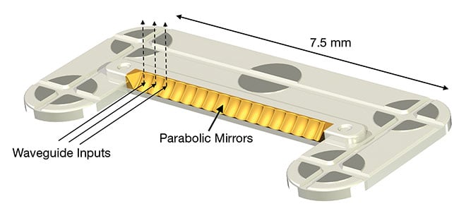
Innovative new vertical coupling methods employ micromirror devices containing parabolic mirrors (top) that can be placed directly into the PCB using passive assembly. This allows the use of VCSELs (bottom) for coupling light into the waveguide layer. Courtesy of vario-optics AG.
Consequently, new initiatives such as the Consortium for On-Board Optics (COBO), have formed to provide a platform for discussion and collaboration for the development of common standards.
The main problem arising from the lack of standards — around component compatibility, for example — still presents a technological and economic barrier to the widespread adoption of CPO and OBO
solutions. Further, although the underlying technological solutions have been around for quite some time, the readiness
level of the component technologies has continued to evolve in recent years. Today, it is increasingly apparent that CPO and OBO concepts have matured enough to finally ring in a new era of board- and component-level photonics that are ready to merge with optical fiber technology and take their place in all photonics networks.
Meet the author
Nikolaus Flöry, Ph.D., is business development manager at vario-optics, where he works on integrated optics applications based on the company’s unique polymer waveguide platform. He holds a master’s degree in physics and a doctorate in optical sciences, both from ETH Zürich; email: [email protected].
References
1. L. Brusberg et al. (2017). Electro-optical circuit boards with single- or multi-mode optical interconnects, in Optical Intercon-
nects for Data Centers. Elsevier, pp. 287-307, www.doi.org/10.1016/B978-0-08-100512-5.00012-7.
2. K. Kim et al. (2022). Multimode waveguide interconnect system design for photonic circuit integration. Consortium for On-Board Optics, www.onboardoptics.org/_files/ugd/7bc1dc_fffcd31ac72e4c5e9b70276c6971623f.pdf.
3. N. Flöry et al. (2021). Highly reliable polymer waveguide platform for multi-port photonic chip-packaging. Proc. IEEE, 71st Electronic Components and Technology Conference (ECTC), pp. 1689-1694, www.doi.org/10.1109/ectc32696.2021.00267.