
On-Chip Tunable Photonic Delay Line Could Help Miniaturize OCT Devices
Scientists at Columbia University have developed an on-chip, tunable photonic delay line to miniaturize imaging technology. Using their on-chip technology to map the back of the eye, the researchers produced high-contrast OCT images and extended the OCT imaging range by 0.6 mm while maintaining a high signal-to-noise ratio. Their work in this area could further the development of hand-held OCT devices for affordable deployment in low-resource settings.
Devices incorporating physical delay lines are used to provide long optical delays with broad bandwidth. Realizing long delay lines while maintaining a low loss and small footprint required the researchers to not only overcome the potential for losses caused by fabrication misalignments between different lithography fields, but also radiation and scattering losses caused by tight bends.
Scientists have used a microchip to map the back of the eye for disease diagnosis. While the interference technology used in the microchip is not new, this is the first time, according to the research team, that technical obstacles have been overcome to fabricate a miniature device able to capture high-quality images. Courtesy of Columbia University.
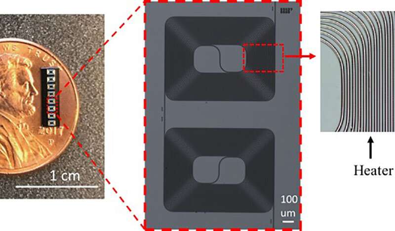
The researchers used a delay line that was 0.4 m in length, coiled into a compact 8-mm2 area using 720 bends, each with a bending radius of only 80 µm. They used a high-confinement silicon nitride (Si3N4) waveguide and tailored the waveguide to be single mode and close to 0 (around 1.3 µm) dispersion.
To allow tunability, the researchers took advantage of the thermo-optic effect of the silicon nitride and designed the waveguides, which are 730 nm high and 780 nm wide, to ensure high thermal overlap between the optical mode and the microheaters. At the same time, the design minimized the loss from the metallic heaters. “By using the heaters, we achieve delay without any moving parts, thus providing high stability, which is important for image quality of interference-based applications,” researcher Xingchen Ji said.
The researchers designed the waveguides to resist misalignments between different lithography fields — a necessary step, since misalignments at the field boundary would increase propagation loss in the waveguide. The team designed the waveguide taper to have a wider width at the lithographic field boundaries, which increased robustness to help prevent misalignment. They fabricated a taper with 5-µm width; and to confirm that the adiabatic taper design helped reduce the stitching loss, they measured the propagation loss of their waveguides across different numbers of fields on the same wafer. The researchers showed that the propagation loss had a linear dependence with the waveguide length, indicating that any additional loss caused by misalignment was negligible.
To demonstrate the capability of the on-chip, tunable photonic delay line, the researchers coupled it with a commercial OCT system. The comparison images taken with and without the tunable photonic delay line using the commercial OCT system showed that the tunable delay line chip did not distort the image.
The on-chip tunable delay line could be applicable to other interference devices. The researchers are beginning to use it to scale lidar systems.
The research was published in APL Photonics (https://doi.org/10.1063/1.5111164).
Published: September 2019