Surface coatings used to control optical, mechanical and electrical properties are deposited as nano- and micrometer thicknesses of special materials.
CERAC, Inc., a subsidiary of Williams Advanced Materials; technical assistance from Pellicori Optical Consulting
Optical coatings are deposited as thin-film multilayers of a variety of materials using specific deposition techniques. Coatings are applied to optical components that are intended for use at wavelength regions between UV and far-IR. The materials and processes used to make these coatings are described here and in the attendant materials data tables.
General material categories and deposition processes
In Table 1, the chemical categories of the materials that are used for optical coating are segregated by spectral region; overlap exists between all regions. Table 2 lists the materials typically used in those spectral regions. These pure (unmixed) compounds represent selections distilled from dozens of potential materials according to required thin-film layer properties such as transparency, mechanical properties, environmental durability and ease of deposition.
TABLE 1.
CATEGORIES OF OPTICAL COATING MATERIALS
Metal Oxide
Compounds
|
|
Multicomponent |
|
Fluoride
Compounds |
|
II-VI and
Semiconductors |
|
Transparent
Conductors |
|
Metal
|
|
| Visible to Near- IR |
|
UV to IR |
|
UV to IR |
|
SWIR to LWIR |
|
Visible to near-IR |
|
UV to IR |
With the exception of the fluoride compounds and lanthanum titanate, these materials are typically deposited by e-beam evaporation or by sputtering from targets. Fluoride compounds and many of the oxide compounds can, alternatively, be evaporated from resistance-heated sources. Because of chemical, stress and process incompatibilities, layers from the oxide and fluoride chemical classes are generally not combined in a coating. The exception is with UV coatings where layers are thin and the material selection of transparent materials is small. Multicomponent materials have been developed to achieve improvements in one or more thin-film layer properties over the single-element precursor. Examples are doped fluorides and oxides and mixtures of two or more similar materials. Mixed and doped starting materials can be obtained, or modifications can be accomplished during evaporation or sputtering from separate sources of materials. Layers of fluorides and sulfides (selenides) are combined in LWIR coatings.
Table 2 also segregates materials according to their mean high-, intermediate- and low-refractive indices within the spectral ranges of greatest usefulness, as limited by absorption. Refractive index is a property of key importance in multilayer coating designs for AR, edge filters, dichroic reflectors, polarizers, laser reflectors and spectral filters.
TABLE 2.
TYPICAL OPTICAL COATING MATERIALS CATEGORIZED BY SPECTRAL REGION AND
REFRACTIVE INDEX INCLUDE PURE FORMULATIONS AND NOT MIXTURES
Wavelength Region
(nm) |
|
Low Index
n < 1.6 |
|
Intermediate
n 1.6 - 1.8 |
|
High Index
n ~2
|
|
| UV: 250 - 400 |
|
MgF2, SiO2, CeF3 |
|
Al2O3, Y2O3 |
|
HfO2, Sc2O3
|
Visible - NIR: 400 - 1100
|
|
SiO2, MgF2 |
|
Al2O3, Y2O3 |
|
Ta2O5, Nb2O5,
LaTiO3, TiO2
|
| UV: 250 - 400 |
|
MgF2, SiO2, CeF3 |
|
Al2O3, Y2O3 |
|
HfO2, Sc2O3
|
SW - MWIR: 1100 - 5000
|
|
SiO2, CeF3 |
|
Al2O3, Y2O3,
SiO
|
|
Ta2O5, LaTio3,
HfO2
|
LWIR: 5000 - 12,000
|
|
CeF3, YF3, ThF4
|
|
-- |
|
ZnS, ZnSe, Ge |
Deposition and growth of thin films of these materials to build optical coatings is accomplished by one of the many variations of two main physical vapor deposition (PVD) processes: evaporation and sputtering. Deposition of films of metal oxide compounds by evaporation or by sputtering can proceed from a preparation of the compound as the starting material or from the base metal and subsequent reactive oxidization to the final desired composition. The nonoxide materials in Table 1 generally start and end with similar compositions. The data tables that follow this article provide suggested deposition parameters.
Coating deposition process technology
• Process outline: The components of the deposition process, from performance requirement to finished product, are diagrammed in Figure 1. It is evident from the descriptions of the process components that material science and deposition technology play complex interdependent roles in successfully producing optical coatings. It is important to understand the individual components and their interactions.
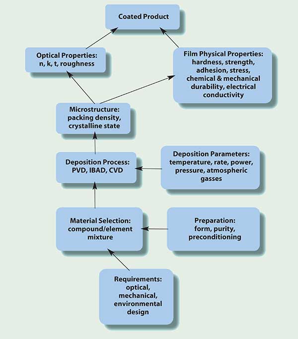
Figure 1. The components of coating materials technology.
• Design and engineering considerations: When presented with the spectral and environmental requirements and the substrate material to be coated, the coating engineer decides on the coating materials and the deposition process and monitoring technique. A thin-film design is generated that includes the wavelength dependencies of the optical constants, refractive index and extinction coefficient, determined for the materals and deposition process parameters. Predicted performance is evaluated with respect to spectral coverage, incidence angle, surface shape, substrate temperature constraints, mechanical durability and verification measurement. The starting form of the coating material and its preparation are selected based on deposition technique and thin-film design. Some materials require preconditioning to prepare for smooth deposition at a constant rate and consistent composition. The deposition process’ operational parameters, previously determined for each material, are programmed into the deposition controller along with the coating design. Deposition parameters coupled with material behavior determine the physical microstructural properties of the thin-film layer. Those film properties in turn determine the optical, mechanical and environmental properties of each deposited layer.
• Materials selections: The materials that will be used in the design are selected according to the spectral criteria of Tables 1 and 2, as well as durability requirements and deposition process. Coating materials are preprocessed and formed to provide controlled vaporization behavior and to insure that the physical and optical properties of the deposited film are consistent from run to run. The optimum film composition, physical structure, and the vaporization behavior throughout the deposition process are strongly dependent on the preparation of the starting material. Furthermore, the different chemical compositions outlined in Table 1 and the specific compounds listed in Table 2 require individual preparations and forms. More detailed discussions are available on the CERAC Web site.1
• Oxide compounds: Oxide films can be deposited from an evaporant source or sputtered using oxide or metallic targets. Evaporable metal oxide compounds are supplied in several forms and preparations depending on the particular compound. Typical physical forms are sintered or melted pieces, broken crystals, hot-or cold-pressed tablets, or pre-melted, preformed e-beam pocket cones. Cold-pressed and sintered preparations of tablets and pellets of various sizes are made from powder that might be combined with a binder and hot pressed in a vacuum or in an inert atmosphere. Compressed density (>95 %) is desired to minimize volume porosity from which water vapor or gas can be released upon heating. Some oxides adsorb surface water; others form hydrates that dissociate with heat. Both types of inclusions can result in the release of water vapor or other trapped gas and generate particulates or cause pressure variations. Fluoride compounds adsorb atmospheric water and experience the same problems and must be gently outgassed.
The chemical state of the starting material might be fully oxidized or be reduced to a suboxide. The reduced state often melts and is conductive; both properties are desirable for e-gun vaporization. Materials that evaporate from the melt have a lower tendency of ejecting microparticulates and spatter (large projectiles) that can result in optical scatter and pinhole creation. When the melt is electrically conducting, e-beam deflection and defocus due to localized charging are eliminated. The reduced forms are gray or black in color vs. white for the fully oxidized insulating material. Reoxidization is achieved in several ways. The first is deposition onto a substrate held at temperature >200 °C, providing an excess of oxygen. The second method is to produce oxygen ions in a reactive plasma process. The third popular technique is to use an ion assist (IAD) source that produces energetic Ar and O ions. If the activation/reactive energies are insufficient to produce a nonabsorbing film, postbaking in air at a high temperature (>300 °C) might be required.
Referring to the tables, we see that the low-index oxide common to all oxide coating combinations is SiO2. The companion high-index materials for visible through SW wavelengths are titania or tantala. A successful replacement for tantala, Ta2O5, is lanthanum titanate LaTiO3. As prepared, this material is actually a complex chemical compound. Compared to pure tantala, LaTiO3 has the desirable properties of requiring lower evaporation temperature producing denser film layers of lower stress with nearly the same index. Its IR transparency extends to ~8 µm.
Titanium dioxide, TiO2, is a favorite visible-range material because of its high refractive index. It finds wide application in AR coatings in the ophthalmic industry. Numerous deposition techniques involving different oxidation states of the starting preparations have been studied. To avoid the presence of multiple and unstable crystalline states in the deposited coating, and evaporation difficulties, the starting material composition should be Ti3O5. This suboxide composition melts, enabling smooth, reproducible deposition. Another high-index alternative to titania and tantala is niobia. Oxides of the three materials can be deposited by sputtering the metal.
Some oxide compounds, and all fluoride compounds, melt before reaching evaporation temperature; others, such as silica, alumina and refractory oxide compounds (hafnia and zirconia), evaporate from a fused vitreous surface or sublimate (SiO). If the material retains its granular form rather than forming a melt, heat transfer among the grains or pieces is inefficient, and the concentration of heat at sharp boundaries such as dust, voids or trapped water sites can result in the explosive emanation of particles and pressure bursts. Extended preconditioning with a sweeping electron beam can reduce these problems.
• Avoiding problems: Particulate showering and spatter and pressure bursts are common problems encountered when evaporating oxide compounds. When the starting material is not properly preconditioned or is of nonoptimum composition, particle emanation can range in intensity from occasional bursts to continuous showering. Particles ranging in size from nanometer to multiple-micrometer can be embedded in the layer and cause light scatter or voids (pinholes) when removed by abrasion. Particulates are often the initiation sites for laser damage and water penetration, and that failure mechanism is as important as absorption in the film in limiting the damage threshold. Included particulates become points of mechanical stress concentration and initiation sites for failures such as crazing and cracking. With underdense starting materials, pressure variation from the release of trapped gases during film layer growth can contribute to inhomogeneity of optical properties as well as upsetting the crystal monitor.
A technique that coating technicians apply to reduce these problems is to create a dense melt by repeated charging of the crucible and melting down to a dense mass. This procedure is wasteful of time and resources, and an improved preparation of many oxide compounds has been introduced: premelted cones that fit the e-beam pocket.
Refractory oxides require evaporation temperatures that range from 1000 °C to >2500 °C to transition from solid to vapor state (see data tables). Materials with evaporation temperatures >2000 °C are tantala, zirconia, hafnia, alumina, yttria and scandia. These materials do not form a melted pool from which evaporation can precede but instead a melted/fused spot – essentially a point source – and the focused electron beam succeeds in eroding a hole whose vapor distribution pattern changes with hole depth. Rapid sweeping of the e-beam should be used to broaden the pattern area, and will reduce thickness and rate nonuniformities. These problems are virtually nonexistent with sputter deposition because of the larger source and higher pressures.
• Controlling nanostructural growth: A growth structure problem common to oxide and fluoride films is that of low packing density. Apart from a small number of exceptions (SiO and alumina), thin films tend to grow with a columnar nanostructure unless special measures are adopted. The energy and chemical environments present during growth determine the nature and scale of the structure. When low energy is present, for example at low substrate temperature, the arriving adatoms do not have sufficient mobility energy to nucleate continuous coverage on the surface. Lacking surface mobility, isolated islands nucleate nanocrystallites that then grow in thickness. Subsequent self-shadowing results in the growth of an open structure of columns that have greater diameters at the substrate surface and taper with height. Vapor incidence at large angles can also increase columnar spacing and exaggerate these problems. The porous structure is not only mechanically weak and soft, but is permeable to moisture. Adsorption of water on the walls of the columns increases the effective optical index and also changes intrinsic stress; both properties are unstable to humid and arid exposure. Spectral shifting and stress-induced failure under varying humidity conditions are evidence of underdense layers.
Film density can increase to near bulklike values by increasing the growth energy of the adatoms or by changing the material composition to discourage singular growth dynamics. In preference to resorting to very high substrate temperatures to eliminate optical and mechanical instabilities, IAD is used to apply high energy to the film. In this technique, ions of oxygen and argon impact the growing film transferring high kinetic energies, ~100s eV. Greater surface mobility and high momentum transfer result in high packing density.
The second method for discouraging low packing density is to introduce an “impurity” content whose species occupy the spaces and the unsatisfied bonds normally accompanying nanocrystallites, thereby interfering with crystalline growth and resulting in an amorphous, dense structure. The additive should be mutually solvent with the host material and possess other favorable chemical properties. A number of oxide (and fluoride) mixtures have been engineered and are available commercially.1,2
Materials that require high vaporization temperatures, such as the refractory oxides, often form multiple crystalline phases. This can occur in the e-gun pocket where the temperature difference between areas can exceed several hundred degrees so that melting and recrystallization occur nonuniformly. The presence in the source of multiple oxidation states and crystal morphologies affects composition and evaporation temperature after repeated evaporations from the same source. The forms possess different refractive indices, stress levels and evaporation temperatures. Therefore, it will be impossible to achieve repeatable results in subsequent production runs without renewing the composition of the evaporation skin layer. This behavior is characteristic of titanium oxide, zirconia and other oxide materials. Critical applications such as wideband AR coatings require that the index of the first thin layer (high index) be repeatable.
• Multicomponent materials: The higher evaporation temperature oxide compounds, zirconia, hafnia and scandia, are transparent into the UV, as noted, but these materials present evaporation and optical problems. A refractive index gradient that varies with film thickness can exist in the film layer. Other oxide compounds, in pure form, suffer inconsistent evaporation behavior. The film itself might contain multiple crystalline states that can transform at high temperature, causing the optical and mechanical properties of the film to be unstable.
Mixed materials composed of a host oxide and small percentage of a similar oxide compound have been introduced to improve on evaporation consistency. In addition, the mixed materials promote the growth of dense film layer structures because the incorporation of the additive discourages the growth of multiple crystalline phases. Instead, a matrix of fine crystallites is assumed to form that is effectively “pseudo amorphous”. The result is stable properties under exposure to high temperature or high energy laser irradiation. Binary and tertiary mixtures have been engineered that exhibit improved hardness and tribological properties along with transparency.1 Lanthanum titanate is a material that provides improved properties, as discussed above.
High mutual solubility exists among refractory oxide compounds namely Al2O3, In2O3, MgO, Y2O3, ZrO2, TiO2 and Sc2O3. The additive proportion is ~10 wt percent. Some examples of available mixtures are TiO2-ZrO2, ZrO2-MgO, ZnS-CeF3. Zirconia is used in laser coatings as the high-index layer. However it suffers from high mechanical stress, inhomogeneous index profile, and low laser damage tolerance. Mixing with 25 percent yttria results in a threefold increase in damage threshold and improved physical properties. Similar results have been reported with hafnia. Adding MgO to zirconia stabilizes the crystalline state to cubic; adding alumina to zirconia constrains the tetragonal state. In these cases, the nanostructure is not amorphous, but is a stable crystalline state. Composing a ternary combination of these compounds results in an amorphous state. The index of mixtures is lower than that for the pure high index component alone.
By varying the relative proportions of a compatible pair of high- and low-index materials, any intermediate index can be deposited to produce an index value that is not available in a single material. Coevaporation, cosputtering and alternating deposition of two sources are techniques used.
• Fluoride coating materials: The evaporation or sputtering of nonabsorbing film layers of oxide compounds requires oxidation to the desired composition by introducing activated oxygen in a reactive process. Fluoride and semiconductor layer deposition proceed without the need to supply components; in fact high vacuum is required to limit gas incorporation in fluoride film layers. Fluorides retain their chemical composition upon evaporation unless excessively high power is applied. It is advisable to operate at a minimum e-beam voltage.
Fluoride compounds are evaporated from a melted or sublimating surface. The fluorides that sublime are prepared by vacuum hot pressing followed by sizing. Melting material forms are crushed premelted or crystalline stock that has been refined by remelting and recrystallization. Fluoride bonds are stronger than oxide bonds so dissociation does not occur with thermal evaporation; however, IAD energies are sufficient to break those bonds and permit partial substitution of oxygen and the generation of oxyflouride compositions. Such compositions are highly absorbing in the UV, however, resulting in lower laser damage thresholds than achieved with pure oxide or fluoride compounds. For this reason, e-beam and resistance heated sources are used without IAD for laser applications.
Many fluoride compounds absorb water and must be dehydrated by gentle heating during the melt preparation. Magnesium fluoride provides the lowest index available over UV to SWIR wavelengths and evaporation material is prepared by precipitation from solution. Substrate temperatures >250 °C are required for the deposition of films with packing density >90 percent. The nanostructure consists of large columns with high void volume. Residual water absorption bands can be detected in the SWIR (~2.9 µm) to MWIR (6.2 µm) regions even for depositions made at high temperatures. The quantity of the volatile component of the absorbed water that resides within the pores changes between humid and arid conditions, causing the index of the film to vary. Yttrium fluoride, transparent beyond the 10-µm wavelength, and other fluoride films also exhibit water bands and index variation. The water bands in ytterbium fluoride, YbF3, are shallower than those in YF3.
Fluoride films typically grow with high tensile stress nature that limits their maximum physical thickness. The coarse growth structure is also responsible for high light scatter from the rough column ends at the film surface. By admixing small quantities of other fluorides, stress, water absorption, and roughness problems associated with the coarse nanostructure are reduced or eliminated. Fluoride mixtures have been in use for many years, some specifically engineered to be nonradioactive replacements for thorium fluoride in IR coating designs. The specific fluoride mixtures that produce dense, amorphous and stable films are CERAC CIROM IRX, IRB and YBaF.1
• II-VI compounds: Optical coatings that operate to wavelengths ~5 µm can be built from the oxide and fluoride materials that we have discussed. Beyond ~5 µm, oxide compounds begin to absorb so sulfide and selenide compositions must be substituted along with semiconductors, as shown in Table 2. A handful of fluorides are also useable up to the limit imposed by thickness-dependent tensile stress level.
The low-index components for MWIR to LWIR coatings, ZnS and ZnSe, sublime and dissociate when evaporated. The starting materials are produced in a CVD process from the reaction of gases. The condensed solids are crushed and sized or pressed into desired working shapes. If substrate surface and chamber atmosphere conditions are favorable, the dissociated components will recombine with correct chemical composition at the substrate and produce nonabsorbing dense films. While e-beam is a useable evaporation technique, a heated baffled box source is preferred because in the nearly isothermal evaporation environment created, there are fewer hot spots that can produce unrecoverable composition deviations.
The high-index component of a LWIR multilayer AR, bandpass, or edge filter is usually germanium, with index = 4, and is evaporated from an e-gun melt. Procedure to obtain nonabsorbing films includes the elimination of oxygen and operation at a deposition rate and a substrate temperature that prevents the formation of an oxide. Silicon can be used for SWIR films, but it is difficult to avoid the formation of a silicon oxide whose evaporation temperature is much higher than that of the metal, and consequently produces spatter.
• Semiconductor materials: Thin-film photovoltaic solar cells using materials alternative to silicon are being produced. Power-generating efficiency is available that is competitive with that achieved by amorphous thin-film silicon. Thin-film layers of direct bandgap semiconductors such as CdTe, CdS and ZnS and multicompositions, Cu(In,Ga)Se2 (CIGS) and CuInSe2 (CIS) or CuInSSe (CISS) are used to construct the absorber layers in PV cells on glass or flexible substrates. Multijunction cells can be constructed by varying the bandgaps of the semiconductors to extend their spectral sensitivity. Evaporation of CdS and ZnS layers is well established technology. Coevaporation or sputtering is used to deposit the CIGS layer (for example). Layers of PV CdS, ZnTe or CdTe can also be grown from a chemical bath in another construction process. The transparent conducting layer is applied over or under the absorber semiconducting layer within the stack that makes up the cell, depending on its character, i.e., its donor function.
• Transparent conducting oxides: Solar cells of all compositions and constructions require a transparent conducting layer as one electrode. Transparent conductors (TCO) are based on the addition to a transparent oxide of a few percent of a cation or anion donor carrier that is responsible for electrical conduction. A variety of TCO materials have been developed; ITO, indium-doped tin oxide, has the longest history and widest application. ITO is being replaced by compositions that are less expensive than indium-containing material. Spray pyrolized SnO2 and SnO2:F are alternates to ITO for solar cell electrodes, as are Cd2SnO4 and Zn2SnO4. Zinc oxide-based formulations and reacted targets of these materials are receiving attention currently. Al:doped ZnO (AZO) is among the TCOs being developed, along with IZO (indium-doped) and GZO (gallium-doped). AZO is deposited by DC sputtering from a target that contains 2 to 4 percent aluminum. Another formulation is Al2O3:ZnO. AZO films are more transparent than ITO films, but less conductive, and material costs are one-third to one-fifth of those for ITO. Lower conductivity is not an issue with transparent electrodes on solar cells. Deposition on cold substrates and easier patterning procedures are further advantages of AZO over ITO.
• Sputtering materials: Sputter deposition has the advantages of reproducibility of results and simple process automation. Optical films can be deposited from a metal target by oxidizing/nitriding sputtered metal ions to deposit an oxide or nitride film layer of the desired composition. DC magnetron sputtering is the technique used with metal targets that are electrically conducting. Oxide (insulating) targets can be sputtered by RF, but the rate is lower. Many variations in the sputter technique have been developed. Practically any material – alloy, mixture, pure metal, ceramic, oxide, nitride, boride, carbide, etc., – can be supplied as a target. Fluorides and sulfides (selenides) are rarely traditionally sputtered because of the hazardous nature of the components and difficulty in maintaining composition.
• Metals: Metal oxide and nitride compounds for optical applications can be deposited by admitting the appropriate reactive gas to the sputtering plasma. Similarly, metal carbide and boride compounds used in tribological coatings can be sputter deposited. High deposition rates are achieved by DC magnetron sputtering. Aluminum, gold and silver can be thermally or e-beam evaporated.
• Use of the materials data tables: The pages that follow list typical deposition parameters for the most commonly used oxide, fluoride and IR coating materials. The materials are available in various forms and preconditioned states; some are intended for evaporation only, others can be obtained as sputter targets. The recommended deposition parameters have been compiled from published sources and personal experience. Because the deposition environment, equipment and tooling are individual to each coating facility, specific adjustment to the recommended parameters is to be expected.
References
1. S. F. Pellicori, CERAC Coating Materials news articles, 1991 to present, and Technical Data Sheets. http://www.cerac.com/ – Technical Publications.
2. http://www.cerac.com/.