Atomic layer deposition allows for conformal coatings on arbitrarily shaped surfaces — and with nanopores, performance capabilities go even higher.
ADRIANA SZEGHALMI, FRAUNHOFER IOF
Today, optical coatings are a commodity: They exist on all types of professional and consumer optics. Among the various technologies for depositing optical coatings1,2, atomic layer deposition (ALD) stands out for its conformal coating on high-aspect-ratio nanostructured and steeply curved surfaces.
ALD is a cyclic procedure in which single atomic layers are grown on surfaces, which allows for precise thickness and composition control. It is a modified version of chemical vapor deposition (CVD), which is still dominant for numerous applications. And with the miniaturization of integrated circuits, ALD is already established in the semiconductor industry.
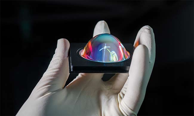
Complex conformal optical coating for a narrow bandpass filter on an aspherical lens. Courtesy of Fraunhofer IOF.
ALD processes are relatively slow compared to other technologies such as evaporation and sputtering, and these techniques are still preferred for optics that have flat substrates. The main advantage of ALD, however, is the conformal growth on curved or otherwise structured surfaces such as gratings or fibers. The single atomic layer is inherently smooth and the method has a high reproducibility.
The ALD process
The ALD process is based on a four-step cycle. An organometallic compound, the precursor of the metal needed, is traditionally used for the final coating. In the first step of the process, a pulse of the precursor material is deposited on a preheated substrate surface. This material generates a chemical reaction with the surface functional groups. Once the functional groups are consumed, the reaction terminates. Second, the excess organometallic precursor and reaction byproducts are purged with an inert gas. In the third step, a second material is pulsed into the chamber, which will oxidize the first compound absorbed on the surface. In general, an oxidizing agent can be water, ozone, or oxygen plasma. Finally, another purging step is applied (Figure 1a).
An important aspect of ALD is that it is a self-terminating process, which means the reaction stops when the surface is saturated at each surface reaction step, leading to atomic monolayers. The deposited thin film has low internal stress and almost the density of the bulk coating material. Inherently, it is also pinhole-free, and the ALD technology is considered the most promising technique for the deposition of demanding barrier coatings for organic photovoltaics and light-emitting diodes. If multilayer stacks are built up for optical application, the cyclic procedure can be repeated 1000× with varying materials, as needed.
ALD is slightly different from most other coating methods, which build their layers with continuous processes, such as physical vapor deposition. Continuous processes have inherent difficulties when making a uniform coating — for example, on curved surfaces and even vertically aligned substrates — whereas ALD will coat them all around (Figure 1b).
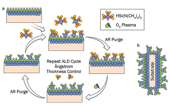
Figure 1. Schema of the ALD process (a). Simultaneously coating substrates on both sides is easily possible with ALD, since the precursors will chemisorb all around (b). Courtesy of Fraunhofer IOF.
Dielectric materials
Typical dielectric materials made with ALD include silica (SiO2), alumina (Al2O3), hafnia (HfO2), tantala (Ta2O5), niobia (Nb2O5), zirconia (ZrO2), or titania (TiO2) as required for interference multilayers made of thin films with high or low index of refraction. Besides oxides, there are several ALD processes available for fluorides, selenides, nitrides, metals, etc. The choice of the materials depends on the desired optical function and the spectral range of interest. Antireflection (AR) coatings require a few layers with a total thickness of several hundred nanometers, whereas more complex interference
coatings such as dichroic mirrors, bandpass filters, or beamsplitters may need coatings up to several microns thick.
An ALD cycle time is approximately
10 seconds or less, but depends on various factors such as the type of substrate and coating material, the type of machine, and the size of the substrate. The typical substrate size in commercial machines
is currently ~200 to 300 mm, but there
are also large reactors — for coating window-size displays, for example. Additionally, the development of spatial ALD reactors allows tens to hundreds of times more rapid growth rates compared to cyclic-type processes.
Although the process of layer deposition is self-limiting, there are small variations in the coating thickness on the surface. Most providers of semiconductor manufacturing equipment or tools guarantee a standard deviation of the ALD coating thickness of 1% to 3% across the substrate, depending on the material and process conditions. Nonuniformities in ALD processes can originate from various causes, such as overlapping precursor pulses because of short purge times, insufficient purging, and nonuniform gas and temperature distributions in the reactor chamber.
Very high uniformity and precise thickness control are essential for optical applications, since deviations from the target values will compromise the optical performance. Using a novel plasma-enhanced ALD tool with a planar triple spiral antenna source, the surface of a
test silicon wafer with a 200-mm diameter is coated with SiO2 and TiO2, and a good uniformity is obtained (Figure 2). The distribution of the thickness deviations is not statistically random, but is well reproducible. The nonuniformity of the film thickness is below 1% for both of these widely applied oxides for optical coatings, even at a very low deposition temperature of 100 °C. Low deposition temperatures are necessary for functional coatings on temperature-sensitive polymer substrates.
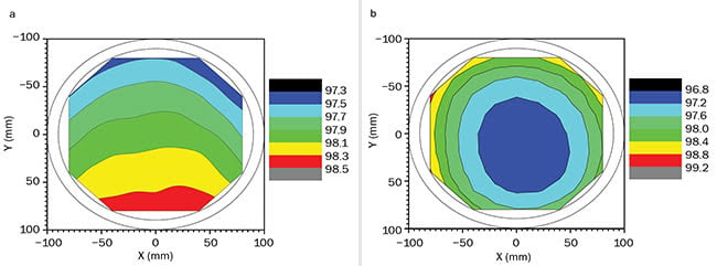
Figure 2. Thickness uniformity of SiO2 (a) and TiO2 (b) thin films deposited at 100 °C and with a novel plasma-enhanced ALD tool for substrates up to 330 mm diameter. The film thickness variation (dmax − dmin)/2daverage is ~0.7% for SiO2 and ~1.1% for TiO2. Courtesy of Fraunhofer IOF.
Curved surfaces
Coating curved surfaces is a challenge, but this is where ALD shows its unique potential. Antireflection coatings are presented here for two different lenses. The reflectivity is measured by means of microspectrophotometry. The first lens, a half-ball fused silica lens with a diameter of 4 mm, was coated with alternating stacks of Al2O3 and TiO2 (Figure 3a), with a top SiO2 layer. In the visible range from 400 to 700 nm, the reflectivity of ~4% of the uncoated lens dropped to ~0.5%. The ALD coating is nearly identical along the entire surface of the lens, despite the very steep curvature of the substrate.
The second lens, a large aspheric lens, was coated with alternating stacks of Al2O3 and Ta2O5, plus an SiO2 layer (Figure 3b)3. The measured spectra fit well with the design curve. Minor deviations on the inclined surface of the lens (positions A and E) may be attributed to a temperature gradient of the lens during deposition and to lateral thickness nonuniformity across the chamber. The nonuniformity of the Ta2O5 layer is ~4%, which already leads to a deviation of up
to 0.5% of the reflectivity.
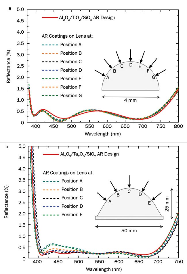
Figure 3. Reflectivity measurements on a 4-mm half-ball lens (a) and a 50-mm aspherical lens (b). Courtesy of Fraunhofer IOF.
Nanoporous SiO2 films
In advanced optical systems, AR coatings should feature very low reflectivity. Theoretical designs have demonstrated the need for very low refractive indices, explicitly much lower than the existing bulk materials. In the case of a single-layer AR coating, the refractive index of the coating must perfectly match the square root value of the refractive index (n) of the substrate. Accordingly, for fused silica or fluoride substrates, layers with n <1.25 are required.
Unfortunately, materials with such a low index of refraction are not available for optical coatings. But nanoporous
(NP) coatings can fulfill this requirement. An NP single-layer AR coating can be made from a stack of SiO2 and Al2O3
layers, where the Al2O3 is removed by
selective chemical etching, leaving NP SiO2 on the substrate. It has been shown that the reflective index of such an NP SiO2 film can be finely adjusted from 1.132 to 1.400 (at 600-nm wavelength) by applying an appropriate ratio between the two components in the composite4. In simple terms, more Al2O3 means more pores and a lower index of refraction (Figure 4).
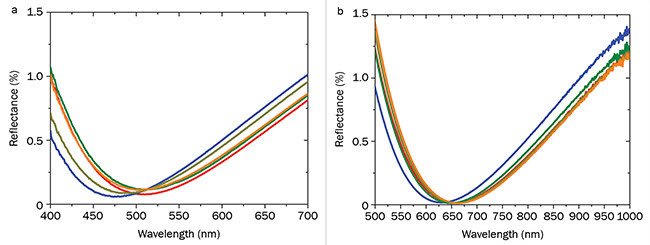
Figure 4. Reflectance spectra of NP ALD coatings on various lenses along the surface of the lens for an AR coating designed for the green wavelength (a) and for the red wavelength (b). The wavelength position of the minimum reflectance can be adjusted by the film thickness. Courtesy of Fraunhofer IOF.
A range of considerations must be made to accomplish real applications. For instance, there is a trade-off between index of refraction of the coating and the porosity: The more pores there are in SiO2, the lower the index of refraction. But more porosity also leads to reduced mechanical stability of the coating. Hence, these coatings are envisioned for coating optics located inside optical systems and not affected by handling.
However, careful choice of the composition and total number of layers of ALD cycles allows a precise adjustment of the refractive index of the NP ALD coating to achieve minimum reflection for a given wavelength. This has been demonstrated for various wavelengths, from 193 nm up to 1064 nm.
The quality of the coatings has been tested by several means. The absorption losses on coatings optimized for 193 and 1064 nm, for example, have been determined to be 430 and 4 ppm, respectively. The threshold for laser-induced damage was tested at 1064 nm and determined to be 92.8 J/cm2, which is close to the damage threshold of the substrate — fused silica in this case.
The wetting properties of the NP coating showed interesting behavior. NP
SiO2 coatings are superhydrophilic, with water contact angles down to 3° to 7° directly after wet etching. A contact angle of 0° means a water droplet would spread immediately over the whole surface. For comparison, the water contact angle of
a bare fused silica substrate was measured at 41° and was still 22° after a 2-hour treatment with H3PO4.
The superhydrophilic effect occurs
independent of the thickness of the coating,
so NP coatings show promise as a finishing coating for many applications where antifogging is important. In addition, low reflectance for a wide range of angles of incidence (AOIs) can be achieved by applying the NP coating as a top layer on a multilayer AR coating5. The reflectance of an accordingly double-sided coated glass substrate is shown in Figure 5. The average reflectance in the 400- to 750-nm spectral range is 0.4% for both AOI 6°
and 45°. Since the absorption and scattering losses of these thin films are very
low, the transmittance of the sample is above 99.5%.
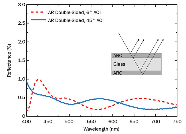
Figure 5. Reflectance spectra measured under AOI 6° and 45° of a multilayer ARC (antireflection coating) with an NP ALD top layer applied to both sides of a glass substrate. Courtesy of Fraunhofer IOF.
Applications now and then
ALD is currently a widespread method in semiconductor manufacturing, often used to create isolating coatings on nanostructures. It can also be used to improve the performance of solar cells or batteries. There is a major potential in using ALD and NP ALD methods to create optical coatings of superior quality on various optical components.
For high-power lasers, NP ALD AR coatings can be tailored to more than
99% transmission and high damage thresholds. But with a few more processing steps, ALD coatings can also be turned into dichroic mirrors, filters, or high-efficiency diffractive optical elements such as transmission gratings.
Due to their unique properties, ALD
coatings can also be applied to other
gratings to create resonant waveguides or polarizers based on ALD-coated nanostructures. The goal is to enable novel optical functionalities not possible on complex-shaped optics before ALD coatings.
Meet the author
Adriana Szeghalmi is a material scientist
with a background in physics and chemistry. She is group leader at the Friedrich Schiller University Jena since 2010 and Fraunhofer
IOF since 2015; email: adriana.szeghalmi
@iof.fraunhofer.de.
Acknowledgments
The author wishes to thank Kristin Pfeiffer, Lilit Ghazaryan, David Kästner, and Vivek Beladiya for their continuous development of ALD processes and optics.
References
1. S. Vandendriesche (Dec. 2016). No one-
size-fits-all approach to selecting optical
coatings. Photonics Spectra, www.photonics.com/Article.aspx?AID=61285&PID=5&IID=917.
2. H. Hogan (Nov. 2018). Optical coating innovations push performance. Photonics Spectra, www.photonics.com/Articles/Optical_Coating_Innovations_Push_Performance/a63972.
3. K. Pfeiffer et al. (2017). Antireflection coatings for strongly curved glass lenses by atomic layer deposition, Coatings, Vol. 7, No. 118, www.doi.org/10.3390/coatings7080118.
4. L. Ghazaryan et al. (2019). On the properties of nanoporous SiO2 films for single layer antireflection coating. Adv Eng Mater, Paper 1801229, www.doi.org/10.1002/adem.201801229.
5. K. Pfeiffer et al. (2019). Wide-angle broadband antireflection coatings prepared by atomic layer deposition. Appl Mater Interfaces, in revision.