Well, now. You’ve read the previous articles covering the ongoing and upcoming trends in lasers, optics and imaging, but you’re probably thinking that there’s more to photonics than those technologies. You are correct; there is much more to the world of photonics. Here’s what is happening in the rest of the industry.
A sense of fluorescence
Whether artificial or from an organic source, fluorescing particles help researchers track biological processes down to the molecular level, for example, or help metallurgists characterize potentially useful new materials. Naturally fluorescent proteins (such as luciferase, typically derived from animals with glowing bits of anatomy) and man-made fluorescent materials, such as quantum dots, can be used as tracers and followed microscopically as they move across a surface. At other times, both kinds can be used as an ersatz flashlight, brought into proximity with nonglowing molecules of interest.
According to Jennifer L. Stow of the University of Queensland in Brisbane, Australia, there are three fluorescence imaging techniques most in demand currently:
1. Real-time imaging in cells and whole animals to visualize fluorescent molecules and cells under physiological and pathological conditions, along with their responses to gene mutations, drugs and others.
2. High-resolution techniques such as stimulated emission depletion microscopy, which permit molecular-level analysis.
3. Multiphoton confocal imaging and total internal reflection fluorescence microscopy, which offers the ability to track multiple fluorophores when analyzing protein localization, interaction and function.
Stow, who is deputy director of research at the Institute for Molecular Bioscience (IMB), located at the university, also notes that fluorescent proteins have an edge for intracellular analysis, but that quantum dots have ever-expanding applications as surface or extracellular probes. The IMB is home to the brand-new Australian Cancer Research Foundation Cancer Biology Imaging Centre.
“The future will be use of proteins and dots in mixtures to provide complex labeling and analysis of cells and membranes,” she said. “Fluorescence imaging is heading toward more colors, higher resolution, faster imaging – all geared toward molecular-level mapping and analysis.”
Spectrometry breakdown
Breaking open a beam of light and reading the resulting spectral highlights as if they were high-precision tea leaves is an age-old technology. Nonetheless, it often is the best way to study subjects from atoms to stars.
Richard A. Larsen of Jasco Inc. says that the greatest interest in the field is centered on Raman spectroscopy.
“The technique is attractive for many reasons,” he said, “and, as the pricing of Raman instruments continues to decrease as a result of technological developments, we expect this interest to continue to increase over the next few years.”
Larsen also sees the use of spectrometry growing in several fields.
“Certainly, the energy sector will have increased demands, particularly for solar energy. As well, the biochemical industries continue to perform research in a number of areas, and spectroscopic imaging instruments are of increasing interest in this area,” he said. “[Jasco is] expecting continued growth in our spectroscopy sales for 2010, with a focus in the research-grade Raman market.”
Taking a position
Any system that incorporates lasers, optics and other precision tools often must include mechanisms for finely controlling the alignment and position of such instruments. Positioning systems, whether mechanical or piezoelectric in nature, get the job done. But are there changes in store in this niche?
According to a pair of leading companies, yes indeed.
Mad City Labs Inc. reports that it is seeing a surge in demand across the board in its positioning products.
“We are seeing active interest in the microscopy/biotechnology markets as well as increased demand in the inspection market,” said the company’s marketing director, Jenice Con Foo, who also noted that the Madison, Wis., company has seen little effect on sales during the recession. “We anticipate increased growth during 2010, not simply based on the economic recovery act, but also as a result of our increased product development, which we have continued during the recession.”
The outlook appears just as sunny at PI (Physik Instrumente) LP of Auburn, Mass.
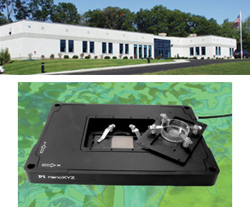
Above, while other companies were laying off people during the downturn, PI invested in onshore design and manufacturing capabilities at its Auburn, Mass., headquarters. Below, the PI nanoXYZ microscope nanopositioning stage is designed and manufactured by PI (Physik Instrumente) LP. According to the company, the stage’s cost, performance and flexibility have made it an invaluable tool for researchers in the bionanotechnology fields. Images courtesy of PI (Physik Instrumente) LP.
“Mechanisms, specialized controllers and software targeted toward life sciences are driving significant new applications and demand,” said Stefan Vorndran, the company’s director of corporate product marketing and communications. “Increasingly, the new generation of piezomotor coarse-positioning mechanisms is necessitated by increasingly stringent stability requirements [for] which this motion technology is uniquely well-suited.”
According to Vorndran and his colleague Scott Jordan, PI has been able to keep investing in the next upswing even during the downturn, instead of laying off highly trained people.
“Tough economic times mean people and processes must work smarter. That means automation. Yields must continually improve. That means precision,” Vorndran said. “And every industry we play in, from microlithography to data storage to photonics to medical design and life sciences, is driven by a continually compressing scale metric and the need for higher speed and throughput. That challenges us to provide better and better nanopositioning equipment at greater and greater values for the next boom.”
Love terahertz
According to X.-C. Zhang, professor at Rensselaer Polytechnic Institute in Troy, N.Y., the most demand for terahertz (THz) imaging is for nondestructive evaluation systems. Suppliers for defense and homeland security are seeking ways to better sense chemical and biological weapons and explosives. Biomedical imaging with THz technology also may provide better diagnoses in a few years.
“In the past, [the] majority of THz research was in the linear spectroscopic measurements which use the relative low THz field strength (<1 kV/cm) as the source,” Zhang said. “With new, intense THz sources recently developed, more nonlinear THz spectroscopic research (such as on dielectric materials measurement with greater than 100 kV/cm or even 1 MV/cm) is expected.”
Zhang predicts that ultrafast THz-based technologies will grow quickly in the next few years, especially emitters with amplified lasers as sources in academic and national labs.
“Coupling high-THz field from free space into local devices, and performing dynamic study of materials could be hot topics,” he said. “Ultrafast technology is the only realistic method to produce high-THz field (>100 kV/cm) with a tabletop system, and there are numerous commercial companies which are providing affordable amplified lasers with mJ pulse energy to generate intense THz waves.”
Slow light speeds up
“I see two exciting developments on the horizon for 2010,” said Thomas F. Krauss, who heads the microphotonics and photonics crystal group at the University of St. Andrews in the UK. “Optical signal processing at ultrahigh bandwidths [is coming], and the ability to tune the delay in slow light structures is improving dramatically. There may well be structures available that offer a tunable delay of up to 100 bits of information.”
Slow light is just what it sounds like, even if it seems a bit counterintuitive at first. Changing the material through which light passes – using a photonic crystal, for example – is one way of slowing it. Bringing light to a more reasonable velocity ultimately will make photonic, rather than electronic, computers possible.
According to Krauss, the strong point about slow light is that it enhances linear and nonlinear photonic functionality with terahertz bandwidth, which likely will lead to applications such as monitoring or regenerating optical signals.
Toshi Baba of Yokohama National University in Japan, who also is working on slow light research, notes that obstacles still remain to making the technology practical. Optical buffers and memory, for example, are still far from practical because they require long delays and high bandwidth with very low loss.
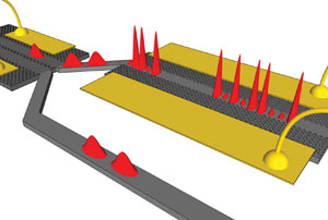
Illustrated here is a slow-light optical buffer. At the entrance, the header is switched out and travels (fast) in the lower branch; meanwhile, the “payload” is stored in the buffer until the header is recognized. This combines the optical signal processing and buffering functions. Both the switch and the buffer are electrically tunable. Courtesy of Thomas Krauss, University of St. Andrews.
Integrating photonics
In addition to slow light studies, the prospects for optically driven communications and computing will depend on integration technologies – the hardware that will enable photons to work hand in hand with electronic circuits.
“In recent years, photonic integrated circuits (PICs) have transformed long-haul optical networks, and we believe PICs also have a tremendous role to play in the future of fiber access networks,” said Steve Bauer of OneChip Photonics Inc. of Ottawa.
According to Bauer, the company sees photonics integration technologies as becoming economically and technologically mandatory in high-volume business and consumer markets, outside of traditional telecommunications.
“We believe that the worldwide economy is starting to stabilize and that system providers and carriers, in 2010 and beyond, will embrace new technologies, such as photonics integration, that will help them deploy FTTx more cost-effectively than ever before,” he said.
Alex Behfar of BinOptics Corp., however, sees it differently.
“For high-volume/low-cost applications, integrated InP photonic chips have not taken any significant market share as of now,” he said. “For example, the vast majority of PON [passive optical network] diplexers and triplexers are still built using discrete InP components.”
Behfar noted that BinOptics, which is based in Ithaca, N.Y., recently introduced a monolithically integrated edge-emitting laser (EEL) and monitoring photodetector (MPD).
“Initially, the EEL+MPD is expected to be used by customers that require the differentiated performance features offered by this product – for example, very tight distribution of MPD current,” he said. “BinOptics sees this as its first high-volume monolithically integrated product, but the level of integration is just two active components – several decades behind silicon electronics.”