As the size of displays grows, array and color filtering challenges increase.
Charles Annis, DisplaySearch
Used in almost every imaginable electronic display application, thin-film transistor LCD modules will generate more than $80 billion of revenue in 2007. Much of the LCD market growth is being driven by flat panels replacing CRT televisions. In 2002, televisions accounted for only 1 percent of LCD module revenues but, in 2007, televisions will exceed 30 percent of revenues. LCDs have been remarkably successful in achieving dominance in the TV market, not only at smaller sizes, but even at the largest sizes, with greater than 100-in.-diagonal models already developed.
For large thin-film transistor LCDs, mass-producing six or eight panels on a single glass substrate is typically most efficient. As demand for larger and larger LCDs continues to grow, manufacturers have increased mother glass dimensions from 680 × 880 mm eight years ago to up to 2200 × 2500 mm now in mass production. Sharp Corp. of Osaka, Japan, recently announced that it will build the world’s first Generation-10 factory, which will use 2880 × 3080-mm glass, targeting production of six-up 65-in. and eight-up 57-in. television panels. LCD equipment makers are rushing to develop Gen-10-capable machines to be delivered in the fall of 2008, so that Sharp can begin mass production in the second quarter of 2009.
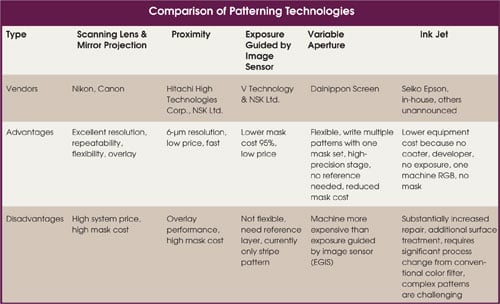
Table 1. A comparison of the patterning technologies shows advantages and disadvantages, along with costs. Total cost factor is all equipment costs over a five-year depreciation period multiplied by the running cost of each machine.
The array and color filter patterning processes create some of the greatest challenges in scaling to Gen 10, in terms of both technology requirements and manufacturing costs. Typical a-Si thin-film transistors have critical dimensions around 3.5 μm and require alignment accuracy of ±1 μm. In color filter manufacturing, only the black matrix step — a black screenlike pattern formed on the color filter that prevents light leakage, improves contrast and separates RGB subpixels — requires less than 10-μm resolution and alignment accuracy of less than ±3 μm. RGB pixels, spacers and vertical alignment protrusions usually do not necessitate resolution precision of less than 20 μm. Although LCD exposure specifications are very loose compared with those of semiconductors, the challenges are in exposing very large areas and maintaining throughput.
The primary method of maintaining productivity as substrates have grown has been increasing the size of the mask and exposure field. The largest masks used in production today for Gen 8 are 1220 × 1400 × 13 mm. With a pellicle — a thin, transparent membrane that prevents particles from contaminating the mask surface — attached, these easily can cost more than $350,000 for a single binary mask. To maintain throughput at Gen 10 and expose 2880 × 3080-mm substrates in four scans, the lithography and mask companies are developing even larger masks in the range of 1600 × 1800 × 17 mm. Initially, these very heavy quartz masks may cost more than $1 million apiece.
In the case of array exposure, average Gen-10 machine prices are expected to be nearly six times higher than those of Gen-4 machines, while the average increase for other tool types likely will be around twice as high. In 2000, lithography costs accounted for only 14 percent of total array equipment spending, but when Gen-10 tools begin shipping in 2008/ 2009, the costs are expected to account for up to 29 percent. For these reasons, exposure is a prime target of cost-cutting strategies.
There are still no alternatives to conventional lithography that are ready for mass production and that simultaneously can meet all the requirements of the array process; therefore, Sharp is expected to adopt a thin-film transistor exposure machine from Nikon Corp. of Tokyo that likely will scale the company’s scanning lens architecture by increasing the number of projection lenses and using a Gen-10 mask to continue to expose nearly 9 m2 of glass in four scans at a cycle time of probably between 70 and 80 s.
Because of less stringent patterning requirements, more of a revolution is taking place in the color filter process, which eventually could eliminate the need for conventional lithography.
Two separate approaches of chaining together multiple low-cost small masks to reduce running costs are being field-tested. The exposure guided by image sensor (EGIS) system developed by V Technology Co. Ltd. of Yokohama, Japan, uses a light source and lens system under the substrate that tracks with a line sensor CCD and that uses a mask/illumination head on the top side of the substrate. Each 300 × 350-mm mask is adjusted in X and Y and rotated based on feedback from the camera system that takes measurements every 5 ms. The constant adjustment allows high-speed 10-μm resolution and 1.5-μm overlay accuracy exposure, which is sufficient for color filter pixels. One concern with the EGIS approach in its current configuration is that it needs a reference pattern on which to align the exposure heads (e.g., black matrix pattern); also, it can expose only repeating patterns such as stripes because the light source is constant.
Greater flexibility in lithography
Dainippon Screen Manufacturing Co. Ltd. of Kyoto, Japan, has developed a separate small mask lithography tool that uses a 308-nm excimer laser, pulsed at 30 ns to expose a variety of patterns via a proprietary, adjustable, overlapping two-mask unit (Figure 1). This configuration allows exposure of a wide assortment of patterns, such as stripes, chevrons, column spacers and circular patterns, at various dimensions. Because of the excimer laser and high-precision stage requirements, the Dainippon Screen machine is thought to be more expensive than the EGIS tool but also to offer greater flexibility. In the future, the company might try to apply variable aperture exposure to array patterning.
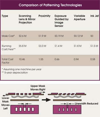
Figure 1. The variable aperture exposure concept uses two masks, an upper and a lower, which allows exposure of different patterns. Source: Dainippon Screen Manufacturing Co. Ltd.
Ink-jet printing of RGB patterns and spacer balls is already in mass production on Sharp and on Tokyo-based Dai Nippon Printing Co. Ltd.’s Gen-8 lines. This process directly prints RGB inks onto color filters and spacer balls in the cell process, without using coaters, exposure or developer machines. Color filter ink-jet printing has proved quite challenging with pinholes and color mixing defects requiring frequent in-process repair steps. Even so, Sharp and Dai Nippon Printing are thought to have dramatically improved the quality of their ink-jet color filters this year and will continue to apply this to Gen 10 for at least half of their color filter requirements.
For Gen-10 LCD manufacturing, a variety of patterning approaches likely will be used in an effort to optimize exposure cost and performance. Although expensive, conventional scanning exposure adopting new masks around 1600 × 1800 mm will remain the dominant method for array patterning because of its high performance and flexibility. Proximity exposure is expected to lose share for RGB patterning but may remain for black matrix and vertical alignment applications. EGIS and variable aperture exposure both potentially offer lower running costs and could be adopted for Gen-10 color filter patterning applications, depending on the results of current beta testing by leading manufacturers. Ink-jet has a very compelling total cost factor, which should make it the primary RGB printing method at Gen 10 and should enable greater adoption at smaller glass sizes.
Meet the author
Charles Annis is vice president of FPD manufacturing research at DisplaySearch in Kyoto, Japan; e-mail: [email protected].