RIVERSIDE, Calif., Oct. 17, 2017 — A prototype developed using quantum mechanical processes could usher in a novel class of ultra-efficient photodetectors that would enable solar cells to turn the light they receive into multiple electrons. The prototype is based on the efficient multiplication of interlayer electron-hole (e-h) pairs in 2D semiconductor heterostructure photocells.
To build the prototype, researchers at University of California, Riverside, stacked two atomic layers of tungsten diselenide (WSe2) on a single atomic layer of molybdenum diselenide (MoSe2). Such stacking resulted in properties that were vastly different from those of the parent layers.
The team observed that when a photon struck the WSe2 layer, it knocked loose an electron, freeing the electron to conduct energy through the WSe2. At the junction between WSe2 and MoSe2, the electron dropped down into MoSe2. The resulting energy knocked a second electron from the WSe2 into the MoSe2, where both electrons became free to move and generate electricity.
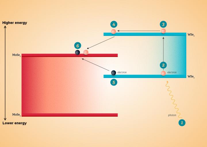
This image shows an energy diagram of the WSe2-MoSe2 device. When a photon (1) strikes the WSe2 layer, it knocks loose an electron (2), freeing it to conduct through the WSe2 (3). At the junction between the two materials, the electron drops down into MoSe2 (4). The energy given off in the drop catapults a second electron from the WSe2 (5) into the MoSe2 (6), where both electrons are free to move and generate electricity. Courtesy of University Communications, UC Riverside.
“We are seeing a new phenomenon occurring,” said professor Nathaniel M. Gabor. “Normally, when an electron jumps between energy states, it wastes energy. In our experiment, the waste energy instead creates another electron, doubling its efficiency.”
Gabor said that understanding such processes, together with developing designs that extend beyond theoretical efficiency limits, could aid in the design of ultra-efficient photovoltaic devices. When the materials used to build the photosensor were thinned down to dimensions close to an electron’s wavelength, the properties of the material changed. In the researchers’ prototype, one photon was able to generate two electrons or more. In conventional solar panels, one photon can at most generate one electron.
“It's like a wave stuck between walls closing in,” said Gabor. “Quantum mechanically, this changes all the scales. The combination of two different ultra-small materials gives rise to an entirely new multiplication process.”
Researchers noted that additional electrons could potentially be generated by increasing the temperature of the device.
Electron multiplication in conventional photocell devices typically requires applied voltages of 10 to 100 volts. To observe the doubling of electrons, the researchers used only 1.2 volts, the typical voltage supplied by an AA battery. By exploiting the highly efficient interlayer e-h pair multiplication process, they were able to show 350 percent enhancement of the optoelectronic responsivity at microwatt power levels in an NIR optoelectronic device.
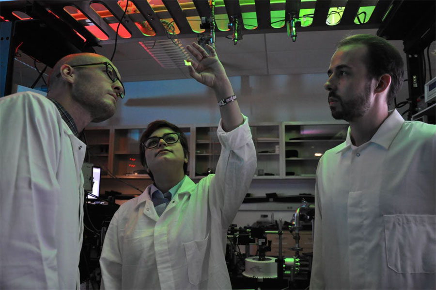
UC Riverside’s Nathaniel Gabor (left) is seen here in his Quantum Materials Optoelectronics lab with his graduate students Fatemeh Barati (center) and Max Grossnickle. Courtesy of I. Pittalwala, UC Riverside.
The findings, which demonstrate efficient carrier multiplication in transition-metal dichalcogenides (TMD)-based optoelectronic devices, could make 2D semiconductor heterostructures viable for a new class of ultra-efficient photodetectors based on layer-indirect e–h excitations.
“Such low voltage operation, and therefore low power consumption, may herald a revolutionary direction in photodetector and solar cell material design,” researcher Max Grossnickle said.
Grossnickle added that the efficiency of a photovoltaic device is governed by a simple competition: light energy is either converted into waste heat or useful electronic power.
“Ultrathin materials may tip the balance in this competition by simultaneously limiting heat generation, while increasing electronic power,” he said.
Gabor believes that the team’s findings could be used in unforeseen ways.
“These materials, being only an atom thick, are nearly transparent. It’s conceivable that one day we might see them included in paint or in solar cells incorporated into windows. Because these materials are flexible, we can envision their application in wearable photovoltaics, with the materials being integrated into the fabric. We could have, say, a suit that generates power — energy-harvesting technology that would be essentially invisible,” he said.
The research was published in Nature Nanotechnology (doi:10.1038/nnano.2017.203).
UC Riverside physicists have developed a photosensor by combining two distinct inorganic materials and producing quantum mechanical processes that could revolutionize the way solar energy is collected. Courtesy of Quantum Materials Optoelectronics lab and University Communications, UC Riverside.