
Photoelectrode Traps, Converts Light Efficiently
A photoelectrode developed by a team at Hokkaido University harvests visible light across a wide spectral range using a semiconductor titanium dioxide (TiO2) layer sandwiched between gold film (Au film) and gold nanoparticles (Au NPs). A key feature of the new structure is that the Au NPs are partially inlaid in the TiO2 layer.
In their quest to develop an energy-efficient photoelectrode, the researchers found that simply applying a layer of gold nanoparticles to a semiconductor did not lead to a sufficient amount of light absorption, because the nanoparticles absorbed light only within a narrow spectral range.
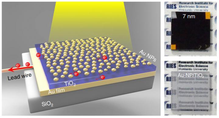
Left: The newly developed photoelectrode, a sandwich of semiconductor layer (TiO2) between gold film (Au film) and gold nanoparticles (Au NPs). The gold nanoparticles were partially inlaid onto the surface of the titanium dioxide thin film to enhance light absorption. Right: The photoelectrode (Au-NP/TiO2/Au-film) with 7 nm of inlaid depth traps light, making it nontransparent (top). An Au-NP/TiO2 structure without the Au film is shown for comparison (bottom). Courtesy of H. Misawa et al/Nature Nanotechnology.
To enhance light absorption, the team sandwiched a 30-nm TiO2 thin film between a 100-nm Au film and Au NPs. When Au NPs absorbed light, the additional energy triggered electron excitation in the gold, which transferred electrons to the semiconductor layer. When the system was irradiated by light from the Au NP side, the Au film worked as a mirror, trapping the light in a cavity between two gold layers and helping the nanoparticles absorb more light in a phenomenon called localized surface plasmon resonance (LSPR). The researchers used strong coupling between a Fabry-Perot nanocavity mode and a LSPR to improve light absorption.
“Our photoelectrode successfully created a new condition in which plasmon and visible light trapped in the titanium oxide layer strongly interact, allowing light with a broad range of wavelengths to be absorbed by gold nanoparticles,” said professor Hiroaki Misawa.
The team found that more than 85 percent of all visible light was harvested by the “golden sandwich” photoelectrode. The new photoelectrode also demonstrated the ability to convert light energy far more efficiently than previous methods.
“The light energy conversion efficiency is 11× higher than those (photoelectrodes) without light-trapping functions,” Misawa said.
The boost in efficiency also led to enhanced water-splitting, a promising process for yielding clean energy.
The researchers believe their approach, which uses very small amounts of material to enable the efficient conversion of sunlight into renewable energy, could contribute to the realization of sustainable energy.
The research was published in Nature Nanotechnology (doi: 10.1038/s41565-018-0208-x).
Published: September 2018