
Photonic Chip Transforms Single Light Beam into Multiple
Researchers at the National Institute of Standards and Technology (NIST) have devised a photonic circuit on a chip that transforms a single incoming beam of laser light into a panoply of new beams, each with a host of different optical properties.
The newly generated beams — which retain the frequency of the original beam — simultaneously exit the circuit at different locations along the chip. That allows scientists and engineers to select the specific characteristics of one or more beams needed for a particular application.
Precision shaping and controlling beams of visible light are critical for diagnosing and studying human diseases, trapping atoms that form the basis of the world’s most accurate clocks, quantum computing, and many other quantum-based technologies.
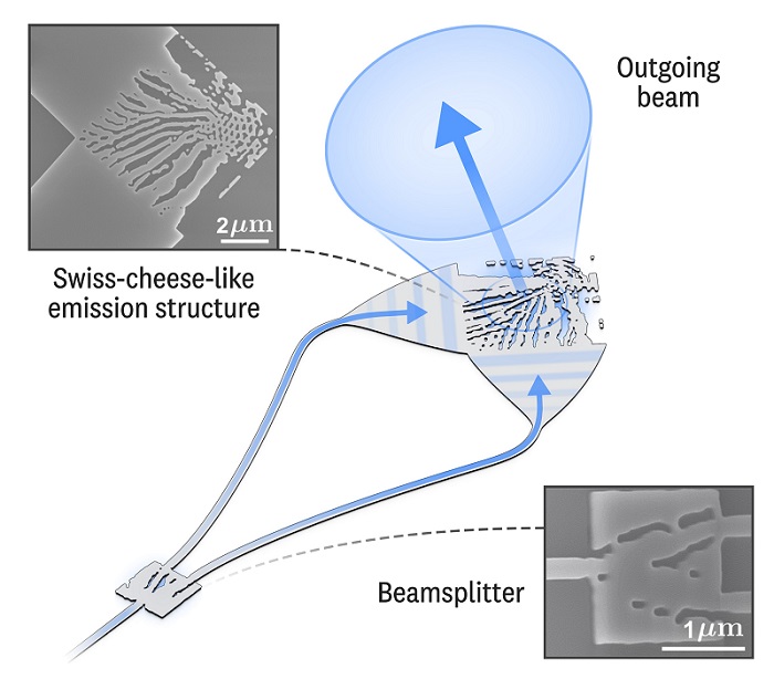
When a light beam enters the photonic chip, it’s guided to regions where a beamsplitter divides the lightwave into two parts. At each location, the Swiss-cheese-like structure of a thin layer of tantalum pentoxide alters numerous properties of the lightwave, including its phase and polarization. Courtesy of S. Kelley/NIST.
Doing so, however, typically requires bulky optics that occupy large amounts of laboratory space. The new NIST-designed device could eventually eliminate the need for such optics and help miniaturize the latest generation of atomic clocks and other devices, enabling their practical use. Small, portable versions of atomic optical clocks could dramatically improve navigation systems, especially underwater, where GPS is not available.
Most methods of shaping and guiding light on a chip, including those that employ metasurfaces, typically convert a single light beam with one set of properties into another single light beam with a different set of properties.
In contrast, “our device can generate a very large number of shaped beams from a single input beam,” said NIST researcher Grisha Spektor. Multiple laser beams that simultaneously bombard a cloud of atoms from different directions are required to trap and cool the cloud so it can be used as the basis of an atomic clock. The newest generation of optical atomic clocks, likely to become the new international standard for defining the second, typically require six laser beams.
The circuit generates these beams within an ultrathin layer of tantalum pentoxide 150 nm thick. Tantalum pentoxide, often employed in optical coatings, has a high index of refraction and is almost perfectly transparent.
Using computer algorithms, Spektor and his colleagues imprinted the tantalum pentoxide layer with Swiss-cheese-like patterns tailored to generate multiple light beams, each with different properties. Because the photonic circuit consists of a single layer of material, it can be fabricated relatively easily and scaled up to larger dimensions as needed, Spektor said.
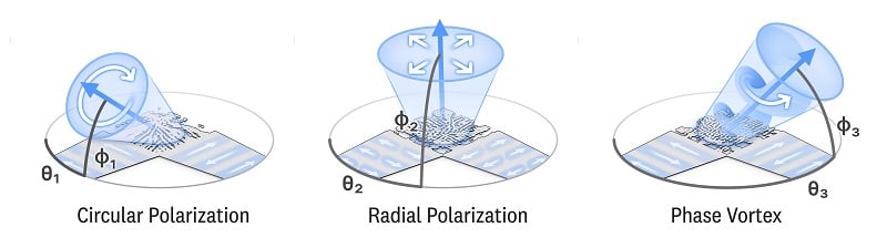
Three examples of how a new photonic chip built at NIST shapes an incoming light beam. A thin layer within the chip, made of tantalum pentoxide, forms a structure that can alter the polarization of an outgoing light beam (plane in which the beam vibrates) depending on its horizontal direction (θ) and elevation above the layer (Φ). The chip can reshape the beam to vibrate in a circular pattern or a radial pattern. In addition, the structure of the material can reshape the beam into a vortex, which alters its phase (the position of a lightwave within its cycle of peaks and valleys). Courtesy of S. Kelley/NIST.
A laser beam enters the chip through a channel that guides the light to several different locations within the chip. At each location, the light stream is split in two. The structure of the tantalum pentoxide imparts a different phase — the position of a lightwave within its cycle of peaks and valleys — to each of the streams.
In addition, the polarization of each of the two split streams — the plane in which the lightwave vibrates — is rotated relative to the other by 90°. The two streams are then recombined and scattered in various ways that create outgoing light beams with practically any desired phase, polarization, direction, or divergence.
Physicists need several wide, or divergent, beams to corral clouds of atoms used in atomic clocks and other quantum technologies. Diverging beams offer another advantage: They can be generated within a tiny region of the chip — less than one-tenth the width of a human hair — enabling the chip to create many closely spaced beams. The small amount of real estate needed to create the beams also leaves the rest of the chip free to perform other tasks and house additional detectors or electronics that a particular experiment or application may require.
The team’s test results show that the chip device, once perfected, should be able to guide, shape, and deliver a virtually unlimited number of closely spaced light beams at a variety of visible-light colors.
The research, conducted in collaboration with Stanford University in California, the University of Colorado in Boulder, and Octave Photonics in Boulder, was published in Optica (www.doi.org/10.1364/OPTICA.486747).
/Buyers_Guide/Octave_Photonics/c33335