VCSELs would be practical in many new applications if they oscillated in a single optical mode. A novel approach to making single-mode VCSELs involves a periodic pattern of holes etched into their top facet.
Paul O. Leisher and Dr. Kent D. Choquette, University of Illinois at Urbana-Champaign
The vertical-cavity surface-emitting laser (VCSEL) has been the subject of intense research since its development in 1977.1 The standard device structure consists of a doped, highly reflective bottom distributed Bragg reflector; an undoped, multiple-quantum-well active region; and a top distributed Bragg reflector with opposite doping. These layers typically are grown by metallorganic chemical vapor deposition. Electrodes are added to the top and bottom distributed Bragg reflectors, and either proton implantation or selective oxidation is used to provide current confinement.2
This design offers several advantages over traditional Fabry-Perot, edge-emitting semiconductor lasers, such as small size, compatibility with on-wafer testing and the fabrication of large arrays, and a round, low-divergence output beam. These features make VCSELs attractive, low-cost laser sources for many near-IR applications, including optical interconnects and gigabit local area networks.
Nevertheless, as a result of the decreasing cost of edge-emitting lasers, VCSEL performance must be improved if these devices are to find new applications. One way in which VCSELs have the potential to outperform edge-emitters is single-mode operation.
Numerous applications require single-mode lasers, including sensing and high-speed optical data communication. Because of their short cavity length, VCSELs inherently lase in only one longitudinal mode. However, reliably achieving single transverse mode operation at high powers requires some work.
Single-mode VCSELs
A common method for fabricating single-mode VCSELs involves the use of a small oxide or implant aperture. Oxide apertures are undesirable for a number of reasons. For one, they provide both current and optical confinement, resulting in less flexibility in the design. For another, the fixed index contrast provided by the oxide layer requires an aperture with a diameter of less than 3 μm, which is difficult to accurately control in fabrication. Optical scattering introduced by the aperture increases the threshold current density, and the series resistance of these devices is high. Finally, the use of these apertures can reduce device reliability.
Conventional single-mode implant VCSELs are somewhat easier to manufacture because the aperture is lithographically defined, but they present other challenges. In this structure, the implant aperture provides current confinement. Transverse optical confinement indirectly results from nonuniform heating caused by the injection-current profile. This thermally induced shift in the index of refraction often is called a “thermal lens.” Single-mode operation typically is achieved for implant aperture diameters smaller than 6 μm, but the thermal lens is unstable and the modal properties somewhat unpredictable.
It therefore is desirable to develop a commercially viable fabrication method that can take advantage of the current confinement properties of oxide or implant apertures and that allow the optical confinement to be independently designed for reliable single-mode operation. In doing so, the sizes of the oxide and implant apertures should no longer affect the modal properties of the device, reducing the tight fabrication constraints and instability issues of conventional oxide and implant structures, respectively.
Meanwhile, another area of active research involves the development of coherent VCSEL arrays. Coherently coupled two-dimensional arrays offer the potential of extended-area coherent sources with high spectral purity, which would be useful in a variety of applications in the high-power (e.g., ladar, optical communications and steerable sources) and low-power (e.g., image processing, spectroscopic sensing and optical logic) regimes.
The ideal 2-D array of coherently coupled vertically emitting lasers would produce an in-phase far-field radiation pattern, with a large percentage of the total output power located in the central on-axis lobe. Efforts to achieve such an array using either evanescent coupling3 or leaky-mode coupling4 have been successful, but they require a difficult fabrication process.
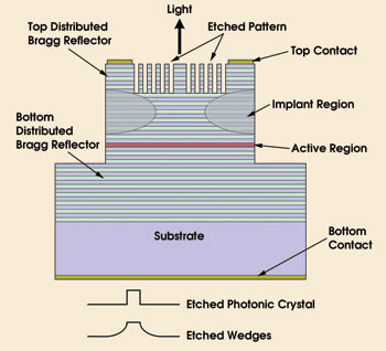
Figure 1. The schematic shows the cross section of a photonic crystal vertical-cavity surface-emitting laser (VCSEL). Current confinement is provided by an implant aperture (shown) or by an oxide aperture. Optical confinement for single-transverse-mode operation is provided by the etched pattern of holes. The effective transverse refractive index profiles for a photonic crystal and holey wedge pattern are shown (not to scale).
Photonic crystal VCSELs
Photonic crystals and other etched holey structures offer a means of realizing both single-mode oscillation and coherent arrays in a way that is compatible with low-cost, high-volume manufacturing, which is crucial to continued commercial success. By etching a photonic crystal with a central defect into the top reflector of the VCSEL (Figure 1), the transverse refractive index profile can be precisely designed to provide single-mode output over the operating range of the laser (Figure 2a). This structure improves on conventional single-mode oxide or implant VCSELs by allowing the transverse optical confinement to be independently defined using standard photolithography. The confinement still is provided by a somewhat larger oxide or implant aperture.
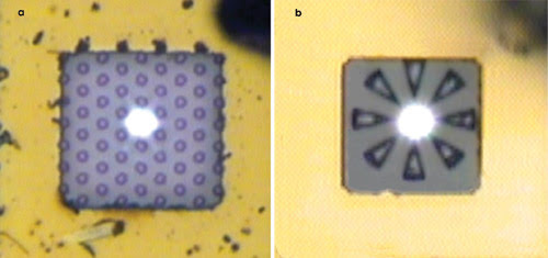
Figure 2. The optical near-field pattern from the top facet is shown for a photonic crystal VCSEL (a) and for a wedge-shaped holey VCSEL (b). Both devices lase in the fundamental mode.
By creating multiple defect regions and by modifying the crystal design between these regions, evanescent coherent coupling of adjacent VCSELs is possible. Additionally, more-exotic etched structures such as wedge-shaped holes (Figure 2b) have been used to control the effective grading of the index in the transverse direction, enabling even higher single-mode powers.
A photonic crystal is created by fabricating a periodic variation in the index of refraction of a material. The devices created by our team at the University of Illinois at Urbana-Champaign rely on the unique out-of-plane propagation properties that the photonic crystal provides, rather than the better-known in-plane photonic bandgap effect. Experimental work has shown that the effective index for a mode propagating out of plane in a 2-D photonic crystal is much higher than what would be predicted by using a fill-factor estimate.5 It is this property that is exploited to fabricate photonic crystal VCSELs.
To design single-mode photonic crystal VCSELs, we use theory originally developed for endlessly single-mode photonic crystal fibers. The basic structure consists of a 2-D photonic crystal with a central defect. The parameters of the crystal, including lattice type, lattice spacing and hole diameter, can be independently chosen to design the index of refraction of the “cladding” region, while the unperturbed index of the central defect forms the “core.”
Given this index contrast and the radius of the central defect (and taking into account the finite etch depth of the holes), photonic crystal VCSELs can be designed to predictably lase single-mode.6,7 Because we dispense with the photonic bandgap effect, the feature sizes of the crystal are not limited by the wavelength of operation, and typical designs have hole diameters greater than 1 μm. Fabrication of the photonic crystal therefore requires only two steps: definition of the pattern by photolithography and a dry etch.
Stable CW operation
Reliable room-temperature continuous-wave single-mode operation has been demonstrated in both oxide- and implant-confined photonic crystal6-9 and holey VCSELs10,11 at a variety of wavelengths. Figure 3 illustrates how a photonic crystal pattern modifies the spectrum of a multimode oxide-confined VCSEL to be single-mode. In oxide-confined VCSELs, the etched photonic crystal or holey pattern usually leads to an increase in threshold and a decrease in efficiency because it introduces loss to the modes confined by the low-index oxide layer as well as index confinement.
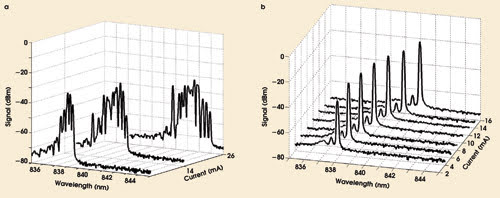
Figure 3. A conventional oxide-confined VCSEL produces a multimode spectrum at various injection levels (a). Etching a photonic crystal into the top facet forces it into single-mode oscillation (b).
In contrast, the index confinement in conventional implant-confined VCSELs is thermally induced and therefore is quite weak. In these devices, the addition of strong index confinement provided by the photonic crystal reduces diffraction loss. This has been shown to simultaneously decrease threshold, increase single-mode output power, increase device efficiency and suppress higher-order modes — that is, the laser improves in every way.
Two main factors have motivated research in symmetric holey structures as an alternative to the periodic photonic crystal pattern. First, because the diameter of the central defect that forms the lasing cavity is a function of the crystal design (i.e., the size and spacing of the holes), it is not a wholly independent degree of freedom in the photonic crystal approach.
Second, the index contrast in theory could be designed to be arbitrarily small so that it would support a single fundamental mode of any desired radius (and therefore power). In reality, there is a lower limit. As the index contrast diminishes (i.e., on the order of 10–3), thermal instabilities cause unpredictable, multimode operation. For 850-nm VCSELs, this limits the maximum reliable single-mode lasing aperture to approximately 10 μm in diameter, which in turn has limited maximum reported single-mode powers to just a few milliwatts.
The use of wedge-shaped holes produces an effective graded, as opposed to step, transverse index profile. This increases the theoretical fundamental mode diameter by more than 40 percent, allowing for a significant enhancement in single-mode output.
To date, we have demonstrated both out-of-phase and in-phase coherent coupling of 2 × 1 and 2 × 2 arrays of defect cavities in oxide-confined photonic crystal VCSEL arrays.12-14 An example of the far-field emission profile is shown in Figure 4.
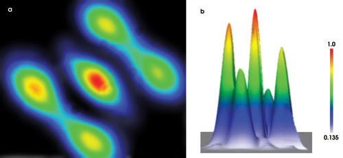
Figure 4. The far-field image of an in-phase coherently coupled 2 × 2 array of defect cavities in a photonic crystal VCSEL shows a central peak surrounded by four minor peaks (a). A height-coded intensity plot depicts the same far-field pattern (b).
Additionally, electronic beam steering has been demonstrated in 2 × 1 arrays by preferentially pumping one defect cavity over the other. By applying antenna array theory to the far-field data, it is possible to calculate the relative phase difference between the fields emitted from each defect.15 It is a change in this phase angle that contributes to beam-steering. Efforts are under way to examine the optical coherence properties of these arrays as well as to explore beam steering.
Etched photonic crystal VCSELs offer great potential for commercialization. They rely on the unique out-of-plane propagation properties of photonic crystals, and as such, the design parameters are not limited by the wavelength of operation. Photonic crystals and other holey structures are designed easily and require only two additional fabrication steps for incorporation into virtually any existing VCSEL design.
Photonic crystal and holey VCSELs may become the low-cost single-mode laser source of choice for a variety of applications. With further research, extended-array coherent sources based on photonic crystal VCSEL technology also may become useful for many applications.
Meet the authors
Paul O. Leisher is a doctoral student (e-mail: [email protected]) and Kent D. Choquette is a professor (e-mail: [email protected]), both in the department of electrical and computer engineering at the University of Illinois at Urbana-Champaign.
References
1. K. Iga (November/December 2000). Surface-emitting laser — its birth and generation of new optoelectronics field. IEEE J SEL TOP QUANT, pp. 1201-1215.
2. K.D. Choquette and K.M Geib (July 1999). Vertical-Cavity Surface-Emitting Lasers: Design, Fabrication, Characterization, and Applications. C.W. Wilmsen, H. Temkin and L.A. Coldren, eds. Cambridge University Press, pp. 193-232.
3. H.-J. Yoo et al (March 26, 1990). Fabrication of a two-dimensional phased array of vertical-cavity surface-emitting lasers. APPL PHYS LETT, pp. 1198-1200.
4. D.K. Serkland et al (Dec. 13, 1999). Two-element phased array of antiguided vertical-cavity lasers. APPL PHYS LETT, pp. 3754-3756.
5. N. Yokouchi, A.J. Danner and K.D. Choquette (September/October, 2003). Two-dimensional photonic crystal confined vertical-cavity surface-emitting lasers. IEEE J SEL TOP QUANT, pp. 1439-1445.
6. A.J. Danner et al (May 2005). Progress in photonic crystal vertical cavity lasers. IEICE T ELECTRON, pp. 944-950.
7. A.J. Danner et al (Feb. 27, 2006). Single mode photonic crystal vertical cavity lasers. APPL PHYS LETT, 091114.
8. H.J. Unold et al (October 2001). Photonic crystal surface-emitting lasers: tailoring waveguide for single-mode emission. Proc. 27th European Conference on Optical Communication, Vol. 4, pp. 520-521.
9. D.S. Song et al (May 27, 2002). Single-fundamental-mode photonic-crystal vertical-cavity surface-emitting lasers. APPL PHYS LETT, pp. 3901–3903.
10. A. Furukawa et al (Nov. 29, 2004 ). High-power single-mode vertical-cavity surface-emitting lasers with triangular holey structure. APPL PHYS LETT, pp. 5161-5163.
11. P.O. Leisher et al (Sept. 1, 2005). Proton implanted singlemode holey vertical-cavity surface-emitting lasers. ELECTRON LETT, pp. 1010-1011.
12. A.J. Danner et al (Sept. 4, 2003). Coupled-defect photonic crystal vertical cavity surface emitting lasers. ELECTRON LETT, pp. 1323-1324.
13. J.J. Raftery Jr. et al (May 16, 2005). Coherent coupling of two-dimensional arrays of defect cavities in photonic crystal vertical cavity surface-emitting lasers. APPL PHYS LETT, 201104.
14. J.J. Raftery Jr. et al (May 2005). In-phase coherently coupled 2-D arrays of defect cavities within a photonic crystal VCSEL. Proc. 2005 Conference on Lasers and Electro-Optics, Vol. 3, pp. 1934-1935.
15. A.C. Lehman et al (Jan. 9, 2006). Relative phase tuning of coupled defects in photonic crystal vertical-cavity surface-emitting lasers. APPL PHYS LETT, 021102.