The symbiosis of manufacturing and photonics is set to change our lives very soon with advances such as 3-D printers and EUV optical lithography.
Conventional lasers of all types are indispensable tools in modern manufacturing, ranging from the classical macro applications of welding, cutting and surface treatment using high-power lasers to the delicate materials processing and PCB via hole-drilling applications using low- to medium-power lasers. Lasers and photonics often are integrated into the complex platforms used in manufacturing processes; conversely, photonic components also are created using these complex platforms. Next-generation photonics requires advances in manufacturing, just as next-generation manufacturing requires advances in photonics.
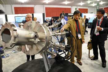
Big guns: Peter Choi, president and director of technology at Nano-UV, unveiled the DPP-based Hydra-12 EUV source for lithography applications at the 2011 SPIE Advanced Lithography Conference in San Jose, Calif.
“To satisfy increasingly demanding manufacturing requirements, laser product technology has to evolve further toward smaller size, lower cost, more-efficient cooling and higher reliability,” said Steve Sheng, president of Telesis Technologies in Circleville, Ohio. “Accordingly, the peripheral laser system technology requires improvement in control electronics, software and fine mechanics.”
Understanding the intricacies of those complex systems and how to integrate lasers into such systems is crucial to bringing the next-generation laser-based industrial solutions to market fruition.
Smaller size
In semiconductor manufacturing, the focus over the next decade is on continuing to reduce the size of transistors per Moore’s law. Although quantum entanglement and optical memory continue to advance in research labs, science has a long way to go before quantum effects will dominate commercial chip manufacturing. In the meantime, a major barrier to making circuits smaller – one that is elusive but very close to fruition – is the production of an extreme ultraviolet (EUV) source for lithography stepper scanners.1 In EUV lithography, an EUV light source exposes the photoresist pattern that creates the circuitry on the silicon wafer. The imaging resolution of a lithography system is limited by the wavelength; the shorter the source wavelength, the smaller the features that can be patterned on the chip. Compared with existing ArF immersion platforms, EUV sources are expected to shrink the size of on-chip features while bringing down the cost per wafer and reducing the fabrication equipment footprint.1,2
Although state-of-the-art EUV lithography platforms with an on-chip transistor density of 22 nm and a 13.5-nm-wavelength EUV source are in the preproduction stage, production volume remains a challenge. A 13.5-nm EUV source must be consistent, reliable, efficient and powerful enough for integration into lithography steppers, while enabling a platform with enough production volume to satisfy high-volume chip producers.3 The other challenge is that glass lenses quickly absorb EUV photons, so the platform must use mirrors instead. The wavefront quality of the optical systems for EUV lithography must be less than λ/30 (0.45 nm rms for λ = 13.5 nm).4 The mirror must be coated with hundreds of layers, each only 3 nm thick. Finally, wafer production usually requires a large vacuum chamber because of the absorption of EUV light in air.
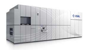
Despite the challenges, commercial platforms are close to reaching the market. Industrial laser producer Trumpf Inc. of Farmington, Conn., focused in the past year on developing a high-power CO2 laser for EUV lithography systems.5 Light-source developers such as Cymer of San Diego and Gigaphoton of Oyama, Japan, offer EUV laser-produced plasma (LPP) sources that use such CO2 lasers. Lithography scanner producer ASML Holdings of Veldhoven, the Netherlands, announced in October the acquisition of Cymer to help speed development of its EUV lithography system. Cymer’s proof-of-concept LPP EUV light sources were demonstrated in laboratories this past summer to expose wafers at a sustained 30-W source power, producing up to 18 wafers per hour (wph). Its next target of 105 W and 69 wph remains a challenge for 2014.6
Other approaches to EUV lithography include that of Eppra (partnered with Nano-UV) of Courtaboeuf, France, a developer whose 13.5-nm EUV Hydra sources are based on a discharge-produced plasma (DPP) technology that uses several multiplexed low-etendue Cyclops sources.7 In 2011, Nano-UV and Eppra unveiled the Hydra, an exceptionally bright EUV light source dedicated to mask inspection, with an irradiance of 1018 photons/cm2/s in the EUV band at the intermediate focus. The source module could form the basic building block of an EUV source through spatial-temporal multiplexing of several units to deliver the brightness and power required for actinic mask metrology.8
Xtreme Technologies GmbH of Aachen, Germany, and Tokyo-based parent company Ushio are pursuing another approach: an EUV light source that combines LPP and DPP into a hybrid called laser-assisted discharge plasma technology.9 In July 2011, the international research institute IMEC in Brussels announced the integration of the laser-assisted discharge plasma source into the NXE:3100 preproduction scanner made by ASML for a pilot manufacturing run. At the 2012 International Symposium on Extreme Ultraviolet Lithography held in Brussels in early October, Ushio announced six months of stable operation of the DPP EUV light source at IMEC. The experiment resulted in a high output power up to 74 W and the claim that 250 W would be feasible.10
In July 2011, the international research institute IMEC (Belgium) announced the integration of a laser-assisted discharge plasma source into the preproduction-stage NXE:3100 lithography scanner made by ASML for a pilot manufacturing run of chips with 22-nm resolution.
In 2013, ASML expects to begin shipping the first of several next-generation NXE:3300:B EUV lithography platforms, with a resolution of up to 22 nm with conventional illumination (18 nm with off-axis illumination). ASML has specified the NXE:3300:B with a productivity of 125 wph. Even if that target is achieved, next-gen EUV lithography platforms are not likely to be a disruptive technology. Chip makers are expected to introduce EUV in a gradual fashion, using it for more difficult critical layers first. When EUV platform productivity improves, reducing the cost per chip, additional layers will be converted to EUV, helping Moore’s law along its way.6
Lighting large
Another growing area of photonics is solid-state lighting, which has seen some changes in manufacturing standards, a trend noticed by Alex Fong, senior vice president of business development for the Life Sciences and Instrumentation Div. of Gooch & Housego in Orlando, Fla. In a recent article, Fong and colleague Alan Tirpak penned a list of changes affecting the manufacturing standards for and regulation of lighting products, such as LEDs and luminaires.11 The introduction of large luminaires using solid-state lighting has changed the testing and quality assurance procedures surrounding LEDs. As manufacturers design and fabricate larger consumer luminaire fixtures, larger integrating spheres measuring 2 and 3 m across are becoming increasingly mainstream.
As larger white LED-based fixtures enter into the consumer product space, Fong said that larger goniometers (to measure angle) coupled with spectroradiometers are required for accurate testing, and thermal radiation becomes a concern with spectroradiometric testing. The Illuminating Engineering Society (IES) of North America has proposed setting new standards, including LM-79, “Approved Method: Electrical and Photometric Measurements of Solid-State Lighting Products,” and LM-80, “Approved Method: Measuring Lumen Maintenance of LED Light Sources,” to address these concerns.
“While the standards are not official per NIST and IES as of yet, such standards are now more or less de facto standard operating procedure,” Fong said. “Until a committee representing the DoE Caliper and LED manufacturers works out the fine details, conducting measurements according to the suggested standards will help facilitate the transition from conventional lighting to solid-state and LED lighting.”
Another trend for the future of manufacturing may be “cold powder molding,” a technique that combines several conventional, mature manufacturing technologies to inexpensively form aspheric surfaces such as lenses. “The thermal infrared spectrum is of interest in nighttime imaging in military, industrial and automotive applications, particularly in the long-wave-infrared region using uncooled bolometer arrays,” said William Plummer, president of WTP Optics in Concord, Mass. “But when designs call for aspheric lenses, conventional manufacturing offers only relatively expensive diamond-turned components or molded chalcogenide glasses.”12 This newly patented approach offers a way to manufacture lenses in high volume for the infrared, out to 20 or even 50 µm in wavelength, with high transmission and a variety of available material properties at very low cost.

Cold powder molding of a US quarter shows minute scratches on a 6.4-mm-diameter area of George Washington’s portrait. Room-temperature potassium-bromide powder was hard-pressed into a solid lens transmitting visible light; such a molded lens can comprise convex, concave and even free-form surface areas with tiny detail and the potential for much larger lenses.
The cold powder molding technique, which involves compression of nanoparticle powders into transparent optics at room temperature, is useful for manufacturing all kinds of lenses, kinoforms, prisms, arrays and other optical components. Any surface shape can be molded, including aspheres and free forms using various optical materials, including inorganic metal halides. The technique is similar to polymer injection molding, but is effective for much longer wavelengths. The technology, currently supported by SBIR grants, is available for licensing.
Cool trends
Besides decreasing size, increasing cooling efficiency is an important aim in industrial manufacturing platforms. Trumpf recently introduced CoolLine, a “cool” new option for its 2-D laser-cutting machines that cools material via a water mist during laser cutting. A special design integrates CoolLine into the laser-cutting head along with nozzles of varied sizes and a water-supply tank. During processing, the CoolLine nozzle directs a cooling mist around the laser beam as it reaches the workpiece, which reduces the heat transfer in the immediate cutting zone. Such cooling enables small sidewalls and difficult contour geometries in thick material, and improves process reliability for low-grade materials and varied-material composition. A cost advantage arises with thick materials because the CoolLine option allows parts to be nested more closely, reducing scrap.13
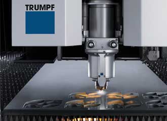
Cool trend: The CoolLine laser-cutting cooling system from Trumpf directs water mist along the laser cut, reducing the heat transfer for more contoured cutting.
Even cooler is the dawning of the “replicator” trend, in which 3-D printers facilitate rapid prototyping of digital designs. A 3-D printer is a tabletop materials printer, enabled by laser and LED technology, that lays down successive layers of polymer or other material – even chocolate – to create solid models. All 3-D printers are driven by CAD-style digital blueprints, often obtained by optically measuring coordinates of an original prototype, according to Morio Onoe, professor emeritus at the University of Tokyo.
The 3-D printer trend is yet another manufacturing technology enabled by photonics. 3-D printers from MakerBot Industries of Brooklyn, N.Y., use LEDs for lighting and digital panels for display; other types of 3-D printers use UV laser beams to harden liquid plastic at the focus. Some use high-power lasers to sinter powder at the focus. The ease of sharing blueprints online combined with the accessibility of increasingly affordable 3-D printers means that just about anyone can instantly create prototypes of just about anything, from jewelry to architectural designs to guns.

3-D printing is another trend enabled by photonics. Shown is the MakerBot Replicator2 3-D printer. How long before there’s one in every home?
On Sept. 18, MakerBot Industries announced the launch of its Replicator2 desktop 3-D printer, which uses fused-filament-fabrication printing technology to create plastic 3-D prototypes.14 Starting at $2199, the Replicator2 can scribe layers as thin as 100 µm into a 410-in.3 volume stage, enabling professional-quality prototypes and models measuring 11 x 6 x 6 in. with dimensional stability – which means that what you design is what you get.
Often compared with early dot-matrix printers, personal computers and mobile phones, these early 3-D printers are likely to improve in performance and decrease in cost, perhaps leading to an entirely new industry with photonics at its heart. “A growing trend with photonics at its core is a good thing for photonics,” Onoe said.
References
1. http://www.cymer.com/euv_lithography/.
2. http://www.euvlitho.com/2010/Keynote-1.pdf.
3. Smoke, mirrors and EUV lithography (March 2011): http://optics.org/indepth/2/3/3.
4. EUV wavefront measurement of six-mirror optic using EWMS (2008): http://144.206.159.178/ft/CONF/16412839/16412921.pdf.
5. http://optics.org/news/3/10/24.
6. http://www.asml.com/asml/show.do?lang=EN&ctx=5869&rid=47397.
7. High-radiance extreme-ultraviolet light source for actinic inspection and metrology (2012):
http://nanolithography.spiedigitallibrary.org/article.aspx?articleid=1352403
8. http://144.206.159.178/ft/CONF/16429058/16429134.pdf.
9. http://www.xtremetec.com.
10. http://www.ushio.co.jp/en/NEWS/ir/20121018_e.html.
11. http://spie.org/x57413.xml.
12. A New Way to Mold Lenses with Freeform and Structured Surfaces. Proc. ASPE, Spring Topical Meeting on Structured and Freeform Surfaces, pp. 11-12 (March 2011).
13. http://www.trumpf-machines.com/index.php?id=49421&L=1.
14. http://www.makerbot.com/replicator2-press-assets.
Moore’s law
Intel co-founder Gordon Moore is credited with the 1965 prediction known as Moore’s law, which states that the number of transistors on a silicon chip will double approximately every two years, while decreasing cost and increasing functionality and performance.
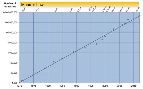
To continue to meet Moore’s law, the dimension of a transistor must shrink about 30 percent every 18 to 24 months. The ability to pattern smaller circuits depends on the wavelength of light used in the lithography process. A shorter wavelength of light can image circuitry with smaller critical dimensions and pitch, which in turn allows the transistors to be smaller and transistor density to increase.
• Moore’s law has driven semiconductor business models and long-term planning
since its inception.
• To continue to meet Moore’s law, the dimension of a transistor must shrink about
30 percent every 18 to 24 months.
• Intel introduced commercial high-volume production of chips in 2011 with a new
3-D transistor structure.
• With features resolved at 22 nm, the 3-D Tri-Gate transistor has tiny transistors
patterned on two sides of a 3-D fin, conserving voltage and power.
• The next target technology node for semiconductor processing is 14 nm by 2014.
• The number of transistors per chip is now approaching 1010, or 10 billion.