Ana Gonzalez, European Photonics Industry Consortium (EPIC)
Market experts in the European Union agree on the need for internet service providers and hyperscale data centers to reach bandwidths of 800 Gbit/s to 1.6 Tbit/s for their users by 2025. To meet this target, industrial suppliers must adopt new technologies, and not all companies are at the same stage of development. This column discusses some of the latest commercial transceivers used for high-speed communications and the technologies that show promise in helping to reach high bandwidths. Also highlighted are companies in the photonics manufacturing supply chain that are working to achieve this goal.
Router connections, client-side optics in the optical transport network, and wireless backhaul (systems that send data from an end user back to a node in the network) have driven the development of higher-speed Ethernet solutions1. This trend is not likely to change, due to increasing consumer demand for video and cloud services. Soon other markets will also require increased bandwidth, such as the automotive industry for connected cars and the electronics packaging industry for the development of harsh-environment packaging solutions.
This increased bandwidth will require the use of cost-effective technologies that can provide the necessary power reduction. In this context, the miniaturization provided by photonic integrated circuits (PICs) makes them the perfect candidate to achieve these goals because they are fabricated on wafers using a standard complementary metal oxide semiconductor (CMOS) fabrication process. Additionally, lasers and other functions can be added by using indium phosphide (InP) and/or hybrid technologies, achieving all the necessary functions in a miniaturized, single platform. Some of the latest commercial developments in optical transceivers use silicon (Si), InP, and hybrid technologies. These transceivers are used in various markets such as last-mile technologies, service providers and hyperscale data centers (long haul, high rate), enterprise, automotive, and automation.
Optical architectures
A standard transceiver is a single-channel device, and each fiber has a single laser source that can transmit up to 10 Gbit/s. However, certain optical architectures can be employed to increase the bandwidth transmitted per fiber, such as coarse wavelength division multiplexing (CWDM), which utilizes multiple channels. A 4-channel CWDM can transmit 40 Gbit/s, and dense wavelength division multiplexing (DWDM) can accommodate up to 100 channels. CWDM and DWDM work via modulation formats such as pulse amplitude modulation 4-level (PAM-4), discrete multitone (DMT), non-return-to-zero (NRZ), coherent quadrature phase shift keying (QPSK), and coherent 8- and 16-quadrature amplitude modulation (8-QAM/16-QAM).
Access technologies
Passive optical networks (PONs) deliver broadband capability to end customers. Currently, for example, PICadvanced, a Portuguese developer of optics and photonics solutions for telecom applications, is focused on creating transceivers for the multiwavelength NG-PON2 (next-generation passive optical network stage 2) technologies based on both discrete and integrated optics. The company, with its integrated optics approach, incorporates all functions on a single chip, resulting in fewer steps in electrical assembly and optical alignment (Figure 1). Building on its Full Photonic Integration InP wafer scale platforms, Netherlands-based EFFECT Photonics has taped out the Manta chip — the world’s first fully integrated coherent PIC targeted at pluggable coherent transceivers for edge and metro/access networks. The Manta PIC is fabricated on EFFECT Photonics’ 3-in. InP platform and will be ported to 4-in. fabrication later this year. It is set to drive a revolution in cost optimization for the next generation of coherent networks (Figure 2).
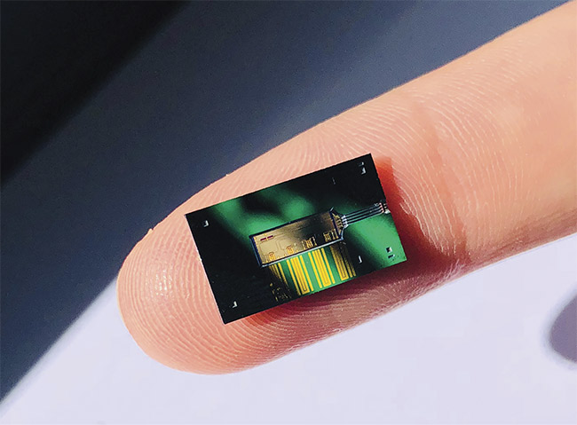
Figure 1. A transceiver on a chip. Courtesy of PICadvanced SA.
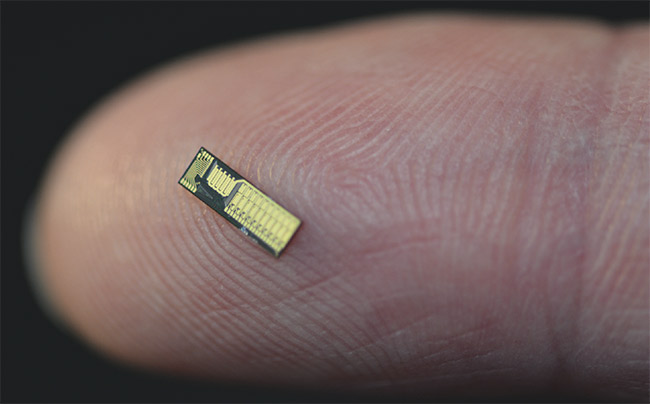
Figure 2. Dense wavelength division multiplexing (DWDM) optical system-on-chip technology. Courtesy of EFFECT Photonics.
Enterprise and data centers
Along with these developments, there is also a need for reduced power consumption and increased reliability in short-distance applications. Some solutions involve Si technologies. For example, Japan-based AIO Core offers its 25-50G NRZ Optical I/O Core (5 × 5 mm). Integrating quantum dot lasers in a Si substrate — and combining photodetectors, waveguides, modulators, transimpedance amplifiers, and optical pins — the Optical I/O Core offers stability under high-temperature conditions. Also, Sicoya, a Germany-based developer of highly integrated silicon photonics, creates Si PICs for optical data centers, with 4- × 25-Gbit/s transceiver chips for intra-data center connections with link distances up to 2 km.
Hyperscale data centers
A high percentage of the 400GbE and faster modules are consumed by a small number of service providers and hyperscale cloud data center operators in the U.S. Many companies are working toward a future beyond 400G transmission, including EFFECT Photonics, which develops highly integrated optical communications products based on its DWDM optical system-on-chip technology.
DWDM dramatically increases bandwidth over existing fiber networks by enabling various data streams to be sent simultaneously over a single optical fiber. Furthermore, because DWDM connections can be amplified, they are able to transmit data across very long distances. The key enabling technology for cost-effective DWDM systems is the use of InP PICs. Efficient laser light sources, waveguides, modulators, and photodiodes also reduce costs.
Optical subassemblies (receivers and transmitters) for DWDM transmission can be obtained separately, allowing more customized solutions. Canada-based Enablence offers arrayed waveguide grating (AWG) wavelength division multiplexers and demultiplexers with 100-GHz channel spacing, packaged with polarization-maintaining (PM) ?bers. The AWG circuit chips are silica and polymer PICs, fabricated using chemical vapor deposition. Additionally, lasers and photodiodes can be integrated onto these PIC substrates.
Horizon 2020’s PASSION project is developing an innovative sliceable bandwidth/bitrate variable transceiver (S-BVT) based on a modular approach to enable multiterabit transmission, while being sustainable in terms of cost and power consumption. PASSION employs low-cost energy-efficient light sources — namely single-mode InP VCSELs from Germany-based VERTILAS — that operate in the C-band. These sources have
a high modulation bandwidth (around
20 GHz) and are directly modulated
using PAM-4 or other multicarrier modulation formats, such as DMT, allowing at least 50 Gbit/s capacity per VCSEL.
The PASSION transmitter basic module integrates 40 VCSELs and
100-GHz spacing multiplexers in a single Si photonic chip (Figure 3), using massive photonic integration to achieve up to 2 Tbit/s capacity per module. Four modules can be tuned by temperature, in a range from 0 to 75 GHz and interleaved with a spacing of 25 GHz, to obtain a 160-DWDM channel supermodule with a total capacity up to 8 Tbit/s. In addition, by exploiting polarization division multiplexing (PDM) and combining two identical supermodules that are orthogonal in polarization, a capacity of 16 Tbit/s can be achieved. Furthermore, space division multiplexing using multicore fibers or bundles of fibers enables the achievement of more than 100 Tbit/s per link. The PASSION transceiver includes a simplified coherent receiver to target distances of hundreds of kilometers.
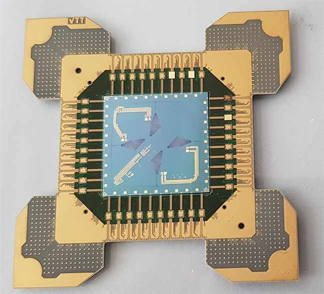
Figure 3. A silicon-based PASSION module design. Courtesy of the PASSION project.
Supply chain is ready
Companies interested in new devices but lacking expertise or having a need to speed up the development process can outsource all required steps — such as PIC design, fabrication, testing, packaging, and large-volume processes — by using the services provided by various companies in the supply chain. Photonic structures can be simulated using a wide variety of software provided by companies such as VPIphotonics; Luceda Photonics; Synopsys; Lumerical; and Mentor, a Siemens business.
However, to speed up the design and optimization process, design houses such as Bright Photonics and VLC Photonics can develop customized PIC circuits. For the production of PICs, it is possible to find foundries that focus on key technologies, such as InP (Figure 4) (SMART Photonics, Fraunhofer HHI, III-V lab, and CST Global), and Si photonics and Si nitride (imec, IMB-CNM, LIGENTEC, ihp, LioniX International, and CompoundTek).
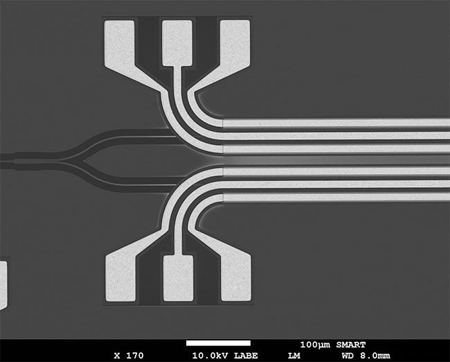
Figure 4. A radio frequency modulator based on indium phosphide photonic integrated circuits (PICs). Courtesy of SmartPhotonics.
Once the prototyping phase has proved successful, thereby validating the optical packages and the design and chip fabrication, it is time to find scalable packaging processes, with focus on automation to reduce the cost of the final device. To help with this, several companies offer packaging solutions for large volumes, such as Netherlands-based PHIX Photonics Assembly. Other companies, such as the Czech Republic-based SQS Vláknová optika, specialize in fiber optics assemblies and optoelectronics. AEMtec (Germany) offers optoelectronic packaging, and AFE (England) offers fiber alignment services, while Nanoscribe (Germany) offers two-photon polymerization processes that can be used to fabricate microlens arrays for coupling light in PICs.
European-based initiatives are helping to accelerate time to market, such as pilot lines in photonics. The JePPIX (Joint European Platform for Photonic Integration of Components and Circuits) Pilot Line offers design, production, and testing services to take an InP PIC-based prototype into production. The initiative lays out a fast open-access route from prototype to commercialization, including interoperability with packaging partners. One such packaging partner is PIXAPP (Photonic Integrated Circuits Assembly and Packaging Pilot Line), which provides companies with standardized packaging solutions for prototyping and pilot-scale production. PIXAPP technology is based on building blocks such as optical coupling and thermal and mechanical stabilization. The initiative aims to drive the future demand for PIC-based products by standardizing processes along the complete PIC manufacturing supply chain. A key goal of PIXAPP is to establish a set of packaging design standards and related design rules that provide users with easy access to well-defined and qualified packaging technologies.
The principal motivation in the development of new transceiver configurations is reducing power consumption while increasing bandwidth using the same fiber. To this end, new devices based on PICs are reaching the market, thanks to miniaturization and multiplexing capabilities. Hybrid technologies that allow the use of CMOS processes but include lasers and detectors via InP integration are also being put to use. Moreover, future developments, including those facilitated by the PASSION project — such as using VCSELs’ massive integration in PICs to dramatically increase the bandwidth per module — may soon be adopted by the industry for further innovations in transceiver generation.
Meet the author
Ana Gonzalez, Ph.D., is currently R&D manager at EPIC (the European Photonics Industry Consortium). Her role is to understand the technologies developed by EPIC members and to identify potential collaborations among the organizations. She also participates in European Commission initiatives such as the various pilot lines in photonics for which she manages business development and marketing strategy. Gonzalez’s expertise is in the development of optical systems and the investigation of applications such as sensing and datacom. She received her bachelor’s degree in chemistry from the University Autonomous of Barcelona and her doctorate from the Catalan Institute of Nanoscience and Nanotechnology.
Acknowledgments
PIXAPP is the world’s first open-access photonic integrated circuit (PIC) assembly and packaging pilot line. It has received funding from the EU’s Horizon 2020 research and innovation program under Grant Agreement No. 731954 (www.pixapp.eu).
JePPIX Pilot Line democratizes access to industrial prototyping and pre-production of high-performance indium phosphide (InP) PICs. The JePPIX Pilot Line is enabled by the InPulse project. InPulse has received funding from the EU’s Horizon 2020 research and innovation program under Grant Agreement No. 824980 (www.inpulse.jeppix.eu).
PASSION is a research and innovation actions project that develops innovative photonic devices and an optical fiber network infrastructure for a sustainable metropolitan network in terms of large capacity, low cost, reduced footprint, and low power consumption. It has received funding from the EU’s Horizon 2020 research and innovation program under Grant Agreement No. 780326, and it is an initiative of the Photonics Public Private Partnership.
Reference
1. LightCounting (2018). High-speed Ethernet optics report (a market report available to EPIC members), www.epic-assoc.com/market-technology.
This content reflects only the author’s view. The European Commission and Photonics 21 are not responsible for any use that may be made of the information it contains.