Femtosecond fiber lasers enable 3D nanoprinting to connect components in the high-volume assembly of hybrid photonic integrated circuits, minimizing alignment requirements.
Jaroslaw Sperling, Menlo Systems, and Matthias Lauermann, Vanguard Automation
Just as electronic integrated circuits have revolutionized
computing, photonic integrated circuits (PICs) are poised to transform applications such as high-speed optical communications, optical signal processing, optical sensing, and quantum information processing.
The vision of unparalleled scalability and automated high-volume production of PICs, enabled by wafer-scale processing technologies of the semiconductor industry, is driving investments of both industry and public institutions. Indeed, high-density photonic integration based on advanced wafer-level processes has been realized for a variety of silicon-based PICs — on the so-called silicon photonics platform.
However, monolithic integration on a single (silicon) chip remains challenging, and most commercial products still must rely on discrete assemblies of photonic chips because, in simple terms, silicon cannot lase.
Using silicon with lasers
Silicon chips can be processed to accommodate various optical functions, but cost-efficient and technically viable
integration of high-performance laser light sources remains difficult. Another class of semiconductor material usually must be used, typically III-V semiconductors such as indium phosphide (InP) or gallium arsenide (GaAs), which poses
a considerable challenge in terms of manufacturability.
One option, referred to as heterogeneous integration, is based on the bonding of III-V chips onto preprocessed silicon wafers. Although well suited for large-scale mass fabrication, the technical
complexity of this approach is considerable. It requires, for example, stringent management of ultraclean and extremely smooth surfaces. Such technological
overhead in many cases conflicts with
the typically short innovation cycles
of PICs.
An alternative option, hybrid integration, involves constructing a PIC using discrete chips made of two or more different materials, to exploit their complementary advantages.
Hybrid integration of laser chips
Hybrid integration relies on optically connecting readily processed III-V components, such as lasers or gain chips, to silicon photonics circuits. The approach maintains the superior performance characteristics of native III-V laser light sources but creates a new fabrication challenge: efficient optical coupling.
Coupling photonic chips is fundamentally more difficult than coupling electronic chips. In electronics, a simple conductive connection is sufficient to guide electrons from one chip to another. Low-loss photonic connections, in contrast, require careful matching of mode field sizes and highly precise alignment to directly couple light exiting the output facet of one chip into the input facet of another chip.
This is particularly challenging for chips carrying high-index contrast waveguides with mode field diameters on the order of 1 µm or less. Assembling such systems has traditionally required active alignment techniques that constantly monitor and optimize the device’s optical coupling efficiency.
Photonic wire bonding, the optical analog to metal wire bonding in electronics, considerably simplifies optical system assembly. Based on 3D nanoprinting of freeform optical waveguides, photonic wire bonding is a variant of additive manufacturing using two-photon polymerization (2PP).
Two-photon polymerization
Two-photon polymerization has been evolving toward industrially relevant applications over the last decade and has been recognized as an enabling technology for photonics, in particular1.
As illustrated in Figure 1, 2PP relies on (laser) light to initiate polymerization of a photoresist within a small voxel (or volume pixel). The photochemistry initiates only upon simultaneous absorption of two photons, with the probability of such an event being nonlinear in light intensity (unlike linear absorption). In practical terms, for a beam of light at a certain wavelength focused into a resist, significant two-photon absorption occurs only in the focal spot, ensuring spatial confinement. Otherwise, the material behaves as quasi-transparent at that wavelength.
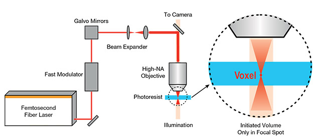
Figure 1. A schematic setup for two-photon polymerization. Femtosecond laser pulses polymerize a small volume of photoresist at the focus, galvo mirrors spatially scan the focus, and a fast modulator adjusts power. Courtesy of Menlo Systems.
By scanning the focal spot spatially, 3D structures of sheer unlimited complexity can be generated with a spatial resolution to 100 nm — well below the diffraction limit of the wavelength employed.
Reliable femtosecond fiber lasers
Because two-photon absorption is orders of magnitude weaker than linear absorption, tightly focused laser beams are the photon sources of choice to drive the process.
In particular, femtosecond lasers delivering pulses with temporal durations on the order of 100 fs have become the workhorses of 2PP.
State-of-the-art fiber-based femtosecond lasers readily deliver pulse peak powers that exceed photopolymerization thresholds.
In fact, the most common requirements in 2PP — in terms of pulse energy, pulse duration, and wavelength coverage — are standard for state-of-the-art femtosecond
fiber lasers that routinely provide nanojoule pulses with pulse lengths well
below 100 fs.
Unlike bulky solid-state laser platforms, femtosecond fiber lasers are small (typically the size of portable devices), they can be thermally managed without external water cooling, and they can be easily integrated via fiber-coupled modular designs (Figure 2).
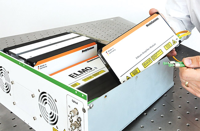
Figure 2. State-of-the-art femtosecond fiber lasers are compact and simple to integrate via fiber-coupled modular designs. Courtesy of Menlo Systems.
Still, their reliability and maintenance-free operation are usually the primary criteria for applications targeting 24/7 operation in industrial settings. These applications demand insensitivity to harsh environmental conditions while delivering high beam quality, excellent pulse-to-pulse and long-term power stability, and spectral reproducibility (Figure 3).
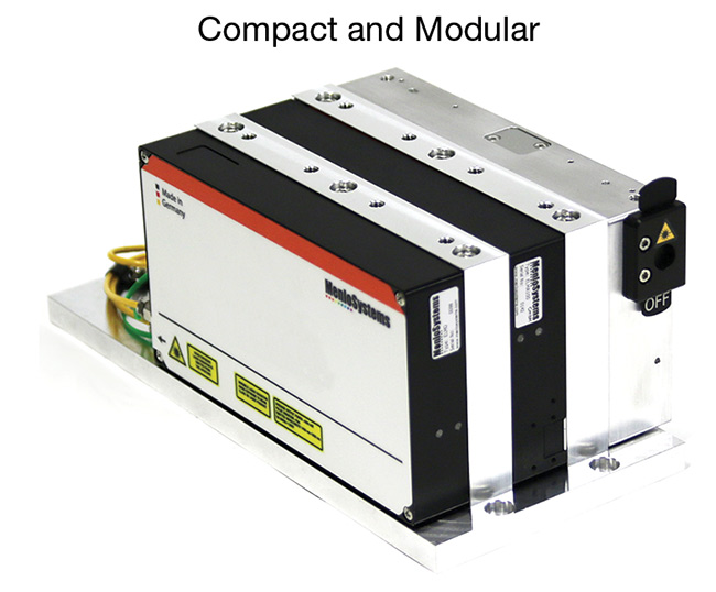

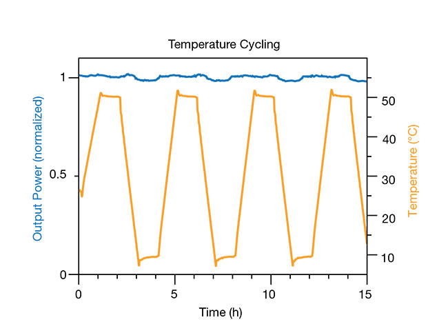
Figure 3. Exemplary performance of an industrial-grade femtosecond fiber laser platform (top) with beam quality (middle) and output power stability under temperature cycling across a range of >40 °C (bottom). Courtesy of Menlo Systems.
These requirements have driven the design of architectures for particularly robust femtosecond pulse generation,
such as the figure 9 design (named after the characteristic shape of the laser cavity)2. The approach uses polarization-maintaining fiber, efficiently decoupling the laser cavity from perturbations such as vibrations and temperature variation,
while eliminating other lifetime-limiting components.
These novel laser developments have significantly advanced practical implementations of nonlinear interactions such as 2PP, which is the heart of photonic wire bonding.
Photonic wire bonding
Figure 4 illustrates the sequence of events in creating photonic wire bonds (PWBs). Discrete photonic chips are fixed to a common carrier, which can be accomplished using standard pick-and-place machinery of moderate precision. The interconnect regions are then embedded into a photosensitive resist, and advanced 3D machine vision detects the positions of waveguide facets and coupling structures with sub-100-nm accuracy. The shapes of the PWB waveguides are calculated on the fly and the PWBs implemented via
direct laser writing using 2PP.
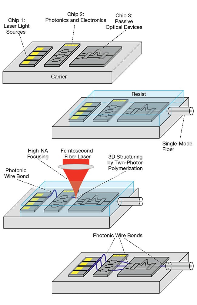
Figure 4. The sequence of steps in photonic wire bonding: Discrete photonic chips are fixed to a common carrier (top). Interconnect regions are embedded into a photosensitive resist (middle, top). Shapes of the photonic wire bond (PWB) waveguides are calculated on the fly and the PWBs are implemented via direct laser writing (middle, bottom). Unexposed resist material is removed (bottom). In a final step, not shown, the PWBs are embedded in a low-index cladding material. Courtesy of Vanguard Automation.
Finally, after unexposed resist material is removed in a development step, the PWBs are embedded in a low-index cladding material, which also acts as an encapsulation for protection against environmental influences and potential contamination.
For chip-to-chip connections, the lateral dimensions of PWB waveguides are typically in the 1- to 2-µm range, with a pitch as small as <20 µm, potentially enabling hundreds of bonds per chip edge in photonic devices (Figure 5a)3,4.
PWBs were found to exhibit remarkable stability with respect to reliability tests including thermal cycling, damp heat, mechanical shock, and vibration3,4. This stability can be explained by the notion that nanoscale structures feature greatly improved resilience with respect to shocks and vibrations as compared with macroscopic or mesoscopic coupling assemblies3. This advantage underscores the utility of PWBs for use cases with stringent reproducibility and reliability requirements4 in nonhermetic operation.
By employing tapered freeform waveguides (Figure 5), photonic wire bonding can cope with vastly different mode fields of the devices to be connected while simultaneously providing low insertion losses over wide wavelength ranges.
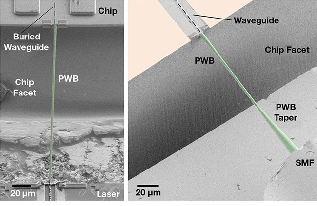
Figure 5. Electron microscopy images of PWBs (above, green) connecting photonic components. PWBs can compensate misalignment of the photonic components and deliver high coupling efficiency using 3D-printed taper structures for mode matching. A PWB connects an edge-emitting laser with a photonic chip (above, left). A PWB connects a photonic chip with a single-mode fiber (SMF) (above, right). Courtesy of Vanguard Automation.
For example, highly efficient coupling
between InP-based horizontal-cavity surface-emitting lasers and silicon photonics chips with coupling losses of <1 dB has been demonstrated3. In these assemblies, the laser sources have been placed alongside the chips, enabling
competent thermal coupling to an under-lying heat sink without consuming on-chip real estate. By compensating misalignments of 20 µm or more, the PWB minimizes alignment requirements for photonic components.
Experimentation confirmed that the photonic wire bonding process does not impair laser performance. Photonic wire bonding has enabled the creation of complete optical communication engines, connecting arrays of InP lasers to silicon photonics modulators and the modulators to single-mode fibers4. Operation of the resulting four-channel coherent transmitter has been demonstrated at a net data rate of >730 Gbit/s, a benchmark for coherent silicon photonics transmitters with
co-packaged lasers.
In addition to photonic wire bonding of multichip assemblies, 3D nanoprinting of microlenses and mirrors lends itself to both die and wafer-level fabrication. This approach limits coupling losses by precise mode matching of optical components with widely dissimilar mode profiles. Moreover, with expanded beams, the alignment tolerances can be relaxed, which simplifies optical system assembly. Micromirrors give additional design freedom and allow the combining of vertically and horizontally emitting components in compact assemblies5.
Accelerating innovation
Packaging and assembly of PICs from discrete chips are major technical and commercial challenges. Photonic wire bonds maintain the performance and versatility advantages of hybrid integration approaches while offering a path toward highly scalable automated mass production. Industrial solutions for in situ printing of photonic wire bonds are emerging, to offer machine hardware- and software-defined functionality for customized processes (Figure 6).
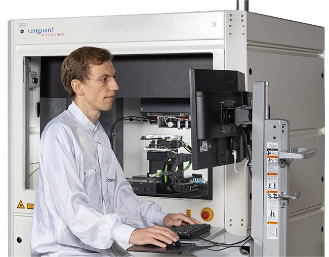
Figure 6. Industrial solutions for in situ printing of photonic wire bonds aim to shorten innovation cycles of photonic integrated circuits and to serve industrial production lines. Courtesy of Vanguard Automation.
Much as electronic integrated circuit development benefited from electrical wire bonding, innovations in PICs are now expected to accelerate. Photonic wire bonding and microlens platforms not only shorten innovation cycles in prototyping but also promise to serve industrial production lines. Inherently robust and reliable femtosecond fiber lasers enable the journey.
Meet the authors
Jaroslaw Sperling, Ph.D., is business developer for femtosecond fiber lasers at Menlo Systems. He joined the company in 2021, bringing his passion and experience gained in various sales- and marketing-related roles across the photonics industry. He has a background in ultrafast laser spectroscopy, and he holds a doctorate in physical chemistry from the University of Vienna; email: [email protected].
Matthias Lauermann, Ph.D., is responsible for the development of automated solutions
for optical packaging using 3D lithography
at Vanguard Automation. He previously was senior development engineer at Infinera Corp. in Sunnyvale, Calif. He holds a doctorate in engineering with a focus on high-speed electro-optical modulators from Karlsruhe Institute of Technology; email: [email protected].
Acknowledgments
The authors wish to acknowledge Christian Mauser of Menlo Systems as well as Sebastian Tobias Skacel and Philipp-Immanuel Dietrich of Vanguard Automation for their assistance in preparing this article.
References
1. T. Baldacchini, ed. (2016). Three-
Dimensional Microfabrication Using
Two-Photon Polymerization. Elsevier,
www.doi.org/10.1016/c2014-0-01016-7.
2. W. Hänsel et al. (2017). All polarization-maintaining fiber laser architecture for robust femtosecond pulse generation. Appl Phys B, Vol. 123, No. 41, www.doi.org/10.1007/s00340-016-6598-2.
3. M. Billah et al. (2018). Hybrid integration of silicon photonics circuits and InP lasers by photonic wire bonding. Optica, Vol. 5, No. 7, pp. 876-883, www.doi.org/10.1364/optica.5.000876.
4. M. Blaicher et al. (2020). Hybrid multi-chip assembly of optical communication engines by in situ 3D nano-lithography. Light Sci Appl, Vol. 9, No. 71, www.doi.org/10.1038/s41377-020-0272-5.
5. P.-I. Dietrich et al. (2018). In situ 3D
nanoprinting of free-form coupling elements for hybrid photonic integration. Nat Photonics, Vol. 12, pp. 241-247, www.doi.org/10.1038/s41566-018-0133-4.