As Moore’s law approaches its limits, advancements in materials science, chip architectures, and quantum technology are opening new paths for electro-optics to enable faster, lower-power computers.
ANDREAS THOSS, CONTRIBUTING EDITOR
Moore’s law has been challenged many times during the past sixty years, but semiconductor engineers always found new tricks to continue doubling the density of transistors on a chip. In the meantime, the cost to do so has skyrocketed. Today, chip makers create structures on silicon chips that are as thin as a few atoms. It will not be long before physics prevents these structures from getting any smaller.
Decreasing the transistor size has always helped to increase the clock rate. There are other ways to enable higher processing speeds, such as cooling or using lower voltages. But most of these methods will also reach their physical limits in a few years, which will inhibit processors from getting faster.
At the same time, the demand for computing power continues to rise, not least due to the advent of artificial intelligence (AI). Furthermore, there is a well-founded demand to limit the power consumption of computer chips, even if the performance of computers or data centers does increase unabated.
Obviously, the problems with electronics amount to basic, physical-level issues, whereas the demand for computing power increases unabated.
Photonics offers potential solutions. We have all benefited from optical fibers replacing copper wires to enable much faster internet in our homes. Light waves have much higher frequencies compared to electronic signals, allowing for higher signal transmission rates. And light waves can be superposed. That is, signals of different wavelengths can be transmitted at the same time in the same fiber.
The ever-faster data transfer opportunities enabled by optoelectronic technology have reached an industrial scale. At the core of this technology are optical transceivers, devices able to both transmit and receive optical signals. Current off-the-shelf optical 400G transceivers transmit 400 Gb/s, and 800G transceivers are now reaching the market. It should be noted that the 400G devices exhibit 100× higher clock rates than the central processing units (CPUs) in a regular office computer.
Transceivers perform an essential role in today’s data centers, where the rate at which data can be transferred is crucial to performance. Currently, they largely connect servers to servers or racks to racks. As soon as a data signal reaches the circuit board within a server, the fiber advantage is lost and transmissions are made electronically. If photonic signals could be brought closer to the CPUs and graphics processing units (GPUs), then data centers would leverage gains in both speed and energy efficiency.
This is easier said than done, however. Photonic data links are much more difficult to manufacture and manage compared with conventional electrical lines.
Onboard optical connections mostly rely on waveguides, mirrors, and coupling schemes that are all alignment sensitive. Poorly aligned or coupled optical components induce signal loss, which makes integrated photonics difficult to package.
Integration of these components on a wafer often leverages traditional CMOS manufacturing processes from the semiconductor realm that have been adapted to the world of photonics. But silicon does not lase and, therefore, integrated photonics solutions require the introduction of unfamiliar materials, such as indium phosphide, silicon nitride, and lithium niobate to provide optical functions. Alternate substrate materials, such as glass, are also under consideration. Intel named Srinivas Pietambaram its 2023 Inventor of the Year for his research on glass as a substrate for computer chips. Glass carries the potential for a 10× increase in interconnect density and integration of optical interconnects. In its announcement about Pietambaram, Intel reported it is working internally and with foundry customers to plan the first products built with a body of glass.
Optical I/O chips off the shelf
The difficulties in efficiently bringing
optical signals to the board and chip level have so far limited the commercial applications for such architectures. But that is beginning to change. Ayar Labs,
a startup based in Silicon Valley, has developed its TeraPHY chiplet for in-package optical input/output (I/O) and is producing it in GlobalFoundries’ high-volume 45-nm fabrication process. In a white paper published by Ayar Labs, the company reports that its chiplet “integrates millions of transistors with hundreds of photonic devices to drive tens of Tbps [terabytes per second] of bandwidth up to 2 km out of the package with unmatched power efficiency of less than 5pJ/b1.” Figure 1 shows an example of how such optical I/O chiplets can be packaged with electronic chips.
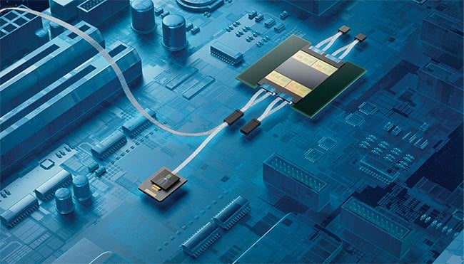
Figure 1. A representative example of how four optical input/output (I/O) chiplets might be integrated into a package with a system-on-a-chip solution. The package connection relies on fiber ribbon arrays. Courtesy of Ayar Labs.
Ayar Labs separated the actual light source, which consists of heat-sensitive laser diodes, from the I/O chiplet and its neighboring heat-producing systems-on-chips (SoCs) (Figure 2).
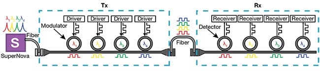
Figure 2. A schematic of Ayar Lab’s multiwavelength SuperNova remote light source attached to the company’s TeraPHY optical input/output (I/O) chiplet (Tx), which sends its signals through a fiber to a receiving I/O chiplet (Rx). Courtesy of Ayar Labs.
The light source, capable of emitting
up to 16 wavelengths, is capable of
supplying light for 256 channels with
a bidirectional bandwidth capacity of
4 Tbps. It is about the size of a smartphone SIM card.
In autumn 2023, Ayar Labs presented
its latest innovation, an optical field-
programmable gate array (FPGA) consisting of two of the company’s optical I/O chiplets connected to a 10-nm FPGA
fabric die, the core fabric used in Intel’s Agilex FPGAs. Two SuperNova light sources power the device’s optical com-
munication and support 64 optical channels across eight fibers on each chiplet. Ayar claims its configuration can deliver 5× more bandwidth at a fraction of the power (<5pJ/b) and latency (5 ns per chiplet + time of flight), positioning it as a potential future solution for data-intensive applications, such as generative AI, machine learning, and novel disaggregated computer and memory architectures.
Optical computers are analog
The concepts described so far illustrate how photonics can speed up data transfer between chips or chiplets. The next question is whether photons can be used to take over central processing tasks.
As soon as a data signal reaches the circuit board within a server, the fiber advantage is lost and transmissions are made electronically. If photonic signals could be brought closer to the CPUs and graphics processing units (GPUs), then data centers would leverage gains in both speed and energy efficiency.
On that point, it is worth taking a closer look at the physical nature of photons and electrons. Electrons carry a charge and, thus, they can be stored in capacitors. When moved, they develop an electromagnetic field that exerts a force on other electrons around. One stream of electrons can be used to control another, which is basically what a transistor does. Most importantly, electrons lose energy while moving, which is dissipated as heat.
None of this applies to photons; they are not susceptible to electromagnetic fields — they have no mass, no charge, and never remain at rest — and do not have optical capacitors or transistors. Because there is not an easy way to build random access memory, there is no simple way to design digital computers with photons.
Therefore, people have considered building analog computers with photons. Analog computers are completely different from the digital desktop systems with which we are familiar. They perform one task, not more, and they do it in real time. For example, a prism performs the Fourier transformation of a beam. What had been a white light signal becomes a spatially separated spectrum after transformation. The process happens in real time, and the precision depends on the detector, not on the prism.
A more complex analog computer is shown in Figure 3. There, a circular coherent laser beam is sent through two subsequent 2D phase masks that act as diffractive optical elements (DOEs). One can imagine the beam as a matrix of beamlets that undergo different phase delays in the two masks. When all the phase modulated beamlets are reunited, they interfere and form an entirely new beam shape, which in the case of Figure 3 is a butterfly.
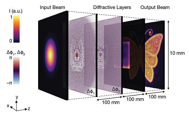
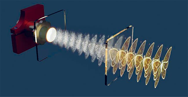
Figure 3. A round laser beam sent through two phase masks is converted into an entirely different shape. Although this setup was developed for beam shaping applications, it offers an example of how an optical configuration can provide the basis for an analog computer that performs a single function. See Reference 2. Courtesy of Carlo Holly.
The butterfly is only an example of the capability to make arbitrary beam shapes. In a real-world setting, this system is used to adapt a beam profile to a laser manufacturing process2. From a mathematical point of view, the DOEs perform a matrix multiplication of their phase-delaying pixels with the respective beamlets. The phase shifts of the pixels correspond to the weights of each node in a neural network and the DOEs represent the network layers. The connection between the layers is established by optical propagation of the light field.
This operation corresponds to the
application of neural networks. Sending
a signal through a neural network is
essentially a series of mathematical
operations per neural layer. Machine learning algorithms help find node weights that lead to an optimal match between the output of the neural network and a given figure of merit.
The beam-shaping setup described is analogous to an analog computer performing exactly one task. The transformation from input to output takes no longer than the time it takes light to travel from one side of the system to the other. Of course, the static DOEs could be replaced by dynamic spatial light modulators (SLMs). This would be appropriate for development tasks or optimization processes. Once the weights (i.e., the phase retardance at each point of the SLM) were defined by machine learning, the analog computer would be operational. This is a typical configuration in applications of neural networks, such as industrial image recognition or even large language models, such as ChatGPT. While the processing of beams in phase masks is visually intriguing and addresses applications in laser materials processing, it cannot be miniaturized easily to the scale of a desktop computer. The way to “real” optical computers requires a different path.
Real optical computers
The benefits that photonics offers in processing speed and transmission rate are so obvious that scientists predicted the advent of optical computers in the 1980s. Researchers at Bell Labs unsuccessfully attempted to create an optical transistor at that time. The problem was, and is, that photons do not interact with each other.
In the 1990s, a wave-based approach evolved based on the interference of two coherent light waves. That is, their fields can add or cancel each other out. This effect depends on the relative phase each wave has to the other, and this can be controlled via electro-optical modulators. Figure 4 shows a Mach-Zehnder-interferometer (MZI), the basic cell or circuit that comprises most modern optical computing systems. In these circuits, two optical waves can be combined, and the phase shifter can impose a phase delay (depending on a tunable electrical signal) on each wave. This phase shift acts as a multiplication between the optical and the electrical signal.
Fast forward: An array of MZIs can perform a matrix multiplication between the light signals and the 2D electric signals applied to all the phase shifters3 (Figure 5).
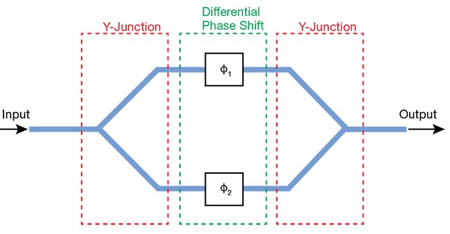
Figure 4. A Mach-Zehnder interferometer (MZI) is a device where one optical input, typically a waveguide, is divided into two arms with adjustable phase delays. When a wave runs through it, the wave splits and the partial waves undergo differential phase-shift delays. When the fields of both waves recombine, their interference produces useful effects. See Reference 3. Courtesy of Lightmatter.
Figure 5. Lightmatter develops systems leveraging Mach-Zehnder interferometers (MZIs) to implement basic linear operations from which much larger matrix multiplications can be scaled. Here, a four-port integrated optical device channels simulated electric field intensity in a directional coupler with optical input at port a. The two adjacent waveguides act like a 50/50 beamsplitter and deliver signals to the exit ports c and d. See Reference 3. Courtesy of Lightmatter.
Since the early 2000s, such devices could be fabricated as integrated photonic circuits on a chip. The setup is almost free of signal losses, and thus it offers high energy efficiency and produces low waste heat, even in a highly integrated version with many MZIs on one chip. In the decade after 2010, a group at MIT’s Quantum Photonics Laboratory not only produced such chips, but they also developed control and readout hardware, and appropriate calibration techniques. Several of the collaborators from that group founded the company Lightmatter in 2017.
Lightmatter mastered a number of challenges that had plagued optical computing, including implementing all of the control and readout circuits on-chip, integrating high-density memory in the package, adding standard electronic communications interfaces to enable external interactions like an electronic accelerator, and building a software infrastructure that made the system plug-and-play for end users.
Lightmatter assembled a proof of concept and built a rack on which two conventional AMD EPYC 7002 worked together with 16 of Lightmatter’s Envise optical chips. The system reportedly can run neural network calculations 3× faster than NVIDIA’s DGX-A100 GPU chip.
Lightelligence, another MIT spinoff, also launched in 2017. The company released its first photonic computing processor in 2021 and is currently building photonic computing hardware based on a silicon photonics platform integrating MZIs. Its latest Hummingbird processor
comprises a vertical stack with an electronic processor on top of a photonic chip, and an optical network on a chip on a PCIe (peripheral component interconnect express) card.
Optical transistors
Several companies have brought optical interconnect to the wafer level and found ways to multiply optical and electrical signals. The drivers for the phase retarders remain electrical. Can this be changed to laser-controlled laser signals? “Yes, this is what we want to do,” said Michael Kissner, founder of the German startup Akhetonics.
The company aims to conquer the holy grail of photonics: a system in which light controls light.
This was declared impossible by the sainted professors at Bell Labs in the 1980s. But science has made considerable progress since then, in terms of packaging as well as materials science.
Akhetonics uses 2D materials, such as graphene, in its pursuit of the grail, Kissner said. These materials have extremely high nonlinearity coefficients, which is what the company needs for optical transistors.
Shining light on such a material changes its optical density for a pulse that traverses the material at precisely the same moment. Akhetonics uses graphene as a saturable absorber, meaning it is black (closed) until a certain intensity is reached and the material becomes transparent to let a subsequent signal pass. Two such switches can be combined to form a gate.
Akhetonics has built a range of different optical gates using graphene on silicon nitride working with the Leibniz Institute for High-Performance Microelectronics IHP in Frankfurt (Oder), Germany for foundry services (Figure 6).
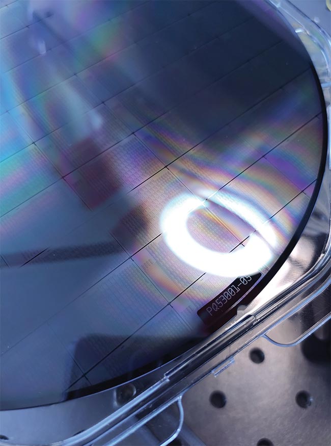
Figure 6. A silicon nitride-wafer carrying graphene-based optical transistors. Akhetonics has built a range of different optical gates using the technology,
with help from Leibniz Institute for High-Performance Microelectronics. To date, the company reports that it has integrated several thousand gates on one 20- × 30-mm chip, offering switching speeds nearing the terahertz level. Courtesy of Akhetonics.
“So far, we can bring up to several thousand gates on one 20 × 30 sq mm chip,” Kissner said. The main benefit is switching speeds up to the terahertz level. “For simple arithmetic operations, we plan to use our all-optical digital-to-
analog and analog-to-digital converters,” he said. “Then we can perform an addition with a simple beamsplitter.”
The company also takes interesting approaches to the storage problem. One is building flip-flop circuits, where the state retains the information. “But that takes too much physical space,” Kissner said. He is more interested in phase change materials.
Strong light pulses can change the phase properties of materials, such as germanium antimony tellurium, to allow short-term storage. Read-only memory — needed for storage of neural network weights, for example — can be fixed in nanostructured polymer structures.
Microsoft’s Project Silica has evolved over the years to offer high-density, long-term optical storage in glass. So, there
are options emerging for pure optical computing, but it will take a few more years of research to exploit their full potential. Akhetonics’ roadmap projects that an all-optical processor will emerge between 2027 and 2028.
Quantum computers
After discussing optical computers, it is not a stretch to consider extending the concept to quantum computing. Of course, an MZI can be used to mix two quantum states. The main difference is
in the generation and detection of the
photonic signals because quantum computers work with single photons.
The challenge for the sources is to produce single photons — most often in pairs — in a deterministic way at high repetition rates.
Detectors for quantum computing systems suffer most from noise; therefore they are often operated at ultralow temperatures.
Nevertheless, the technology is seen as promising and, accordingly, a report from Forbes quoted high valuations for quantum computer companies, such as its $3.2 billion valuation for PsiQuantum, a startup in Palo Alto, Calif.4 The company is developing optical quantum computers
and plans to achieve 1 million qubits on one chip.
This claim is supported by PsiQuantum’s partner GlobalFoundries, a giant in the semiconductor industry. Together they have developed a unique manufacturing process for optical quantum computers on a chip, incorporating interferometers, splitters, and phase shifters. The partners included superconducting nanowires in their fabrication processes for the detectors. Having control of the optical processor relies on advanced electronic CMOS control chips with ~750 million transistors.
Additional companies currently working on optical quantum computing include QuiX Quantum in the Netherlands, Xanadu Quantum Technologies in Canada, Quandela in France, and a number of U.K.-based companies such as TundraSystems Global and ORCA Computing.
Summary
Optical technology is increasingly
deployed in computing applications, leading to more processing power and less power consumption. Researchers are pursuing several different approaches to develop this technology. For example, developing photonic interconnects can speed up the connections between conventional chips to Tbps data rates, and innovating optical processors based on Mach-Zehnder interferometers can take over specialized computing tasks,
particularly for AI applications. Still, others are leveraging photonics to build quantum computers. So far, however, most optical computers are directly connected to electronic control systems. But pure optical calculators are under development too. It may just take a few more years until they arrive in regular computing systems.
References
1. Ayar Labs Inc. (December 2021). Technical
Brief: Optical I/O Chiplets Eliminate Bottlenecks to Unleash Innovation, p. 4.
2. P. Buske et al. (2022). Advanced beam
shaping for laser materials processing based on diffractive neural networks. Opt Express, Vol. 30, No. 13, pp. 22798-22816.
3. M. Gould. (2019). Lightmatter blog post on Medium.com. Optical Components for matrix processing, www.medium.com/lightmatter/optical-components-for-matrix-processing-73687cdd7aa6.
4. Forbes (September 2022). PsiQuantum Has a Goal For Its Million Qubit Photonic Quantum Computer To Outperform Every Supercomputer On The Planet, www.forbes.com/sites/moorinsights/2022/09/21/psiquantum-has-a-goal-for-its-million-qubit-photonic-quantum-computer-to-outperform-every-supercomputer-on-the-planet/?sh=512110bc8db3.