ELENA BELETKAIA and JOSE POZO, EUROPEAN PHOTONICS INDUSTRY, CONSORTIUM (EPIC)
The NewSpace movement focuses on solutions compatible with low-orbit satellites that can provide new applications in the areas of telecommunications and sensing. NewSpace is mainly being driven by innovative launcher, satellite, and technology developments (funded by private companies) that originate from “Old Space,” or traditional, government-funded innovations made by agencies such as the European Space Agency (ESA). The major objectives of NewSpace include lidar, ladar and radar for space, free space optical networks, low-light cameras and sensors, quantum technologies, and integrated photonics innovations. All of these topics were addressed recently during the “EPIC Meeting on New Space” in September that took place at ESA in the Netherlands. Representatives from ESA talked about the current role of photonics in the space industry, the achievements that photonics has enabled, and the needs and expectations regarding the technologies.
Lidar technology for space
The importance of photonics technologies has already been proven for ESA space programs and missions. In the summer of 2018, Atmospheric Dynamics Mission Aeolus was launched by ESA as a lidar mission. The Atmospheric Laser Doppler (Aladin) instrument on board Aeolus is based on UV lidar and uses the Doppler effect on the backscattered laser lights to measure the wind speed and accumulate wind profiles. It has been returning a wealth of useful data on winds in the atmosphere, data that is being used for updating weather prediction models in Europe.
Other lidar applications in NewSpace are related to orbital robotics in medium-size satellites, including refueling missions, space debris removal, and satellite pose estimation. The applications are also significant for scientific uses such as planetary exploration and rover navigation. While gathering data for a critical application such as navigation, a lidar system must have long-term utility, and it should also provide high resolution in real time. Direct contact with sunlight cannot be avoided; thus lidars in space must work when sunlight shines directly on the lens of the optical system. Simulations are necessary to see whether the range and other parameters will be reliable in the worst conditions.
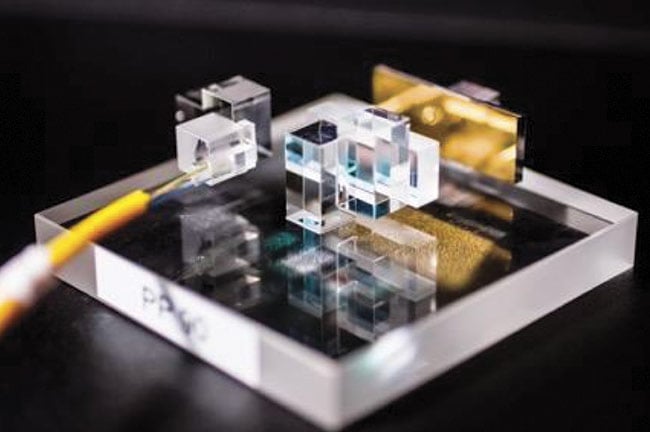
Figure 1. Multiplane light conversion technology. Courtesy of Cailabs.
Many approaches can be taken in the development of lidar imaging systems. Some are based on mechanical scanning, which has many advantages, but certification can be difficult due to the moving elements because high-precision optical components can be sensitive to vibration.
Flash-based approaches and other methods encounter problems with range during daytime conditions and with low spatial resolution. For measuring systems based on the reflection time process using light pulses of varying intensity in the nanosecond range, First Sensor offers highly sensitive avalanche photodiodes (APDs) with internal amplification across a wide dynamic range and bandwidth. To achieve the high spatial resolution required in lidar systems, First Sensor develops APD arrays that consist of multiple sensor elements using, for example, 8, 16, 5 × 5, or 8 × 8 pixels.
Another approach is to use MEMS-based scanners, but the diameter of the entrance pupil and therefore the range usually present a challenge. A system by Beamagine revolves around a patented full solid-state design based in MEMS with a range of 20 m at 10% reflectivity. The maximum distance from the target is 80 m and at least 30 m of range is reached in the worst conditions of direct sunlight simulation. Also, the system features the same resolution in horizontal and vertical access, as well as two imaging modes. One imaging mode can detect the typical range image, while the other can detect the energy of the backreflective pulse and gives additional information on the reflectance of objects within the field of view. Finally, the system’s solid-state design lidars do not include internal moving elements and they have the required certification and robustness.
While lidar technology has contributed to progress in the automotive industry, it is gaining its position within NewSpace for such critical tasks as proximity navigation, robotic approach support during refueling missions, space debris removal, and planetary exploration.
While lidar technology has contributed to progress in the automotive industry, it is quickly gaining its position within NewSpace for such critical tasks as proximity navigation, robotic approach support during refueling missions, space debris removal, and planetary exploration.
Why we need lasercom
While 4G transmission (with 5G coming soon) and an excellent connection with the internet are available almost all the time, fiber still cannot be put into airplanes or satellites. So an alternative way to communicate with them is needed. There is not enough bandwidth to bring the information generated down to Earth because the amount of data produced by satellites and within airplanes is growing quickly. The current estimate is that 30% of the information generated from Earth observation systems cannot be brought down to the ground. With the growing need for the transfer of information, laser communications systems offer many benefits. Lasers offer better SWaP (size, weight, and power), an unlicensed spectrum, and high security. Additionally, they can increase the throughput, and hence reduce the cost in bits per second. However, two main challenges exist: Lasers require tight PAT (pointing, acquisition, and tracking) and they are impeded by the atmosphere.
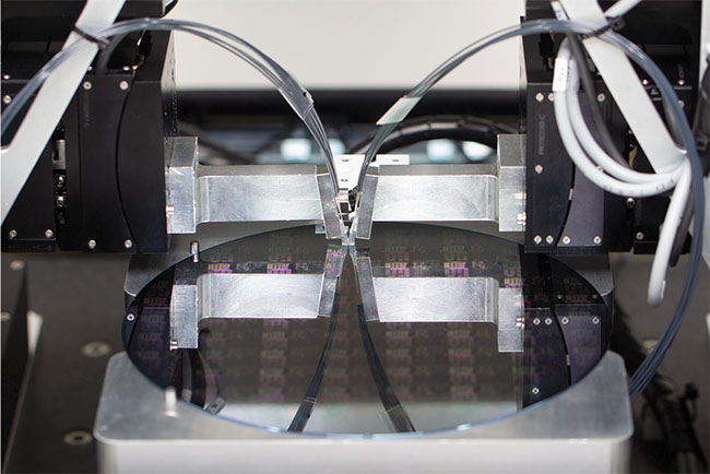
Figure 2. Twin multifiber optical probes of an automated wafer-level tester system for on-wafer photonic integrated circuits. Courtesy of the Silicon Photonics Group, ORC, University of
Southampton (UK), and ficonTEC Service GmbH.
One function required in space is the spatial multiplexer. It enables the splitting of inputs arriving from the multimode fiber into several single modes while keeping the selectivity, or while sending fundamental modes coming into one output and going into a second output, and so on. Cailabs offers tools to handle the shape of light, addressing multiple shapes of light at the same time, splitting them into different fibers, or combining them together. The tools are derived from quantum optics’ multiplane light conversion (MPLC) (Figure 1). This technique enables passive optical beam shaping with no intrinsic loss and no moving elements, and the complex beam shaping is realized through a succession of spatial phase profiles. In a real demonstration, up to 45 modes can be split. MPLC can be used as a transmission tool. It can remove pointing errors between satellites since, when the beam is displaced, MPLC will generate many automodes. Another application of this technology is the mitigation of the atmospheric turbulence. Mitigating turbulence at reception is important because sometimes a concentration of light will reach the detector, while other times there will be no light at all, as the light may have been scrambled or is at zero. One solution includes adaptive optics; however, the moving parts make this solution less durable, and it can be expensive because it requires high-speed mid-infrared cameras in telecom wavelengths. The alternative is to split the turbulence into modes and program the operation on the outputs.
While photonics can substitute for radio frequency transmission and provide possible solutions to overcome cloud issues for laser communications, the resistance of the optical components to shocks, vibrations, and various kinds of radiation
needs to be tested. And photonics interface standardization in the industrial community needs to be established.
Quantum technologies and PICs
Quantum technology is a fast-developing industry with applications in computing, sensing, communication, and metrology. Quantum communication and quantum metrology help in establishing secure cryptography and navigation accuracy, respectively, and use rubidium and ytterbium (Yb) ions.
A Yb-ion-based clock includes many transitions, and the electrons must be moved around at various energy levels,
which means that a lot of lasers are involved. Several wavelengths are also needed to move the electrons to the correct position. One of the repump transitions is a forbidden transition and is completely insensitive to the external environment. It runs in the same frequency on Earth and in space, in hot or cold air, so it is always the same, and this is why it can used as the clock reference. While the best mechanical clocks have an accuracy of one second per year, an optical atomic clock has an accuracy of one second per the age of the universe. Such quantum clock technologies push toward greater precision in many space applications, including inertial sensors, magnetic and gravity field measurement, and geodesy. To enable an optical atomic clock, an extremely stable and narrow linewidth (an atomic transition linewidth in hertz or megahertz) laser source is required. The linewidth laser must also be tuned to the transition of the atom of interest.
Patented BRaMMS (Bragg Range Michelson Mode Selector) technology developed by UnikLasers Ltd. ensures long-term wavelength stability. Single-mode operation is obtained through the use of a volume Bragg grating and Michelson interferometer within the cavity. Stabilization is then provided by the tilt locking method. This technology was applied in a project in which lasers targeting strontium and rubidium absorption lines used in atomic clocks were developed with an output power of up to 80 mW. As part of another consortium of companies, TOPTICA Photonics AG is leading the laser development of a transportable high-availability and easy-to-use optical single 171Yb+ ion clock that can be operated outside a specialized laboratory.
The current challenge is to miniaturize
the optical clocks to enable their inclusion in satellites in space and other applications. One company, vario-optics AG, offers miniaturized and lightweight optical systems for high-speed signaling and sensing, as well as replacement of electrical solutions, enabling reduction of power consumption, increased bandwidth, and
protection against environmental influences. Further integration of smaller lasers such as all on-chip lasers at wavelength, as well as a size reduction in the bulky optics, could be enabled by photonic integrated circuits (PICs).
Besides the advantages of miniaturization, PICs offer automatized tools for ramping up the volume of products based on indium phosphide chips (Figure 2). New fabrication techniques based on ultrafast laser inscription enable higher precision, while the development of new materials makes it possible to avoid surface contamination on space devices.
As these examples illustrate, photonics technology is being worked into space missions. To ensure rapid, game-changing innovations for the future and for the photonics industry, it is important for NewSpace and Old Space to maintain a close link. They should move on parallel lines, both benefiting from the cooperation between institutional missions and privately funded NewSpace missions. Photonics can contribute by shortening
the time to launch, thanks to higher production rates and cheaper technology, smaller sizes, and fewer needs for testing, thus shortening the cycle of innovation. According to the ESA, developments in photonics will enable missions tomorrow that are not possible today.
Meet the authors
Elena Beletkaia, Ph.D., is project leader at the European Photonics Industry Consortium (EPIC). She graduated from Lomonosov Moscow State University, where she specialized in biophysics. In 2015, Beletkaia received a doctorate from Leiden University, where her research focused on biochemical and biophysical mechanisms underlying the metastasis of Ewing sarcoma. Later, in the collaborative setting of NKI (the Netherlands Cancer Institute) and the University of Twente, she investigated the application of noninvasive spectroscopic/multiphoton methods for intraoperative resection margins assessment. All of Beletkaia’s research projects have involved the understanding and use of multiple microscopic and spectroscopic techniques.
Jose Pozo, Ph.D., is the director of technology and innovation at the European Photonics Industry Consortium (EPIC), with close to two decades of experience in photonics technology. He has a doctorate in electrical engineering from the University of Bristol in England, and bachelor’s and master’s degrees in telecom engineering. Pozo is a member of the board of the IEEE Photonics Society Benelux.