The global photonics community’s signature showcase in San Francisco was bigger than ever in 2024. Contributing editor Andreas Thoss examines some trends, and an expedition, from his itinerary.
BY ANDREAS THOSS, CONTRIBUTING EDITOR
On February 1, the biggest North American photonics convention concluded. It was busier than ever, with over 24,000 registered attendees.
Guests once again enjoyed a great reunion for the photonics family, and, beyond a meet and greet event for the community, Photonics West again featured an overwhelming number of events: conferences with thousands of presentations, short courses, four distinct exhibitions (another record), and many, many parties.
Though it is impossible to cover such a wealth of information, a few points topped my personal Photonics West 2024 agenda.
Secondary Sources
The topic of secondary sources has been around for some time. Now, the engagement of one of the biggest players in the laser industry, TRUMPF, is driving further momentum.
To understand the motivation for secondary sources, one must first look at the primary sources, namely the big accelerator facilities (think DESY, in Germany, and Stanford Linear Accelerator [SLAC], in California). The brilliant x-ray sources that these facilities offer are widely used for research, principally in biology and materials science, and disciplines in which particle acceleration, for example, dominates R&D pursuits. Beam times at these primary sources are almost always overbooked. Their use cases for basic and applied research are a core driver for the development of smaller and more energy-efficient (secondary) sources.
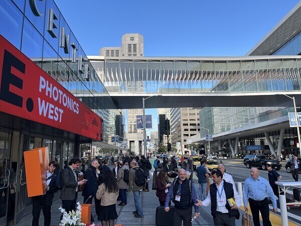
Photonics West 2024 welcomed 24,000 registered guests to San Francisco, with technical advancements, as well as industry and market forecasts, driving record attendance. Courtesy of Andreas Thoss.
Monday at Photonics West, the day bridging the close of the BiOS exhibition and the start of the Photonics West exhibition, offered a chance for an expedition outside of San Francisco. This year, a tour to SLAC brought me to the very place where thousands of bright people do research and “explore the universe at its biggest, its smallest, and its fastest.”
At SLAC, a Department of Energy (DOE) national lab operated by Stanford University, I met with Mark Hogan, director of the Facility for Advanced Accelerator Experimental Tests (FACET-II). This SLAC-located, next generation secondary source is built to determine how new accelerators might become much smaller sources.
Here, electrons are accelerated and forced to emit intense, short x-ray pulses. This happens in an accelerator that is several miles long. Hogan’s research centers on plasma wakefield acceleration (PWFA), a concept that might lead to 100× shorter accelerator schemes. The concept is well distinguished from laser wakefield acceleration (LWFA). Electron bunches in the PWFA realm are unrestricted by the laser repetition rate, and thus better adapted to the existing accelerator schemes.
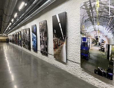
An underground photo gallery at Stanford Linear Accelerator (SLAC) shows the actual beauty of technical installations. Courtesy of Andreas Thoss.
The FACET-II source was completed only recently and is in its first year of regular operation, producing sub-femtosecond pulses of bright x-rays. These isolated attosecond pulses, with microjoule energy and high brightness, are used to explore elementary processes in materials science and biology. These pulses can resolve elementary electronic and configurational processes nobody has seen before.
Back at Photonics West, the advancements at FACET-II led to a discussion with Hagen Zimer, CEO for laser technology and member of the managing board of TRUMPF SE. TRUMPF, as Photonics Spectra covered in its spotlight on secondary sources last year, has applied pulsed x-rays to aid in the understanding of the fine details of copper welding processes for e-mobility. Now, the company wants to apply its extensive knowledge in laser sources to build secondary sources.
It is worth mentioning that this is not an altogether new undertaking for TRUMPF. The company’s existing secondary source technology already earns the firm roughly $1 billion per year, due to a laser system that it delivers to ASML, which turns radiation from a huge CO2 laser into extreme UV (EUV) light at 13.5 nm. Zimer said that the company plans to use its solid-state laser systems to build sources for x-rays, proton beams, and even neutron beams.
Zimer confirmed that TRUMPF has developed secondary sources for different research projects funded by the German government: “One is a laser driven x-ray source; another is a high-harmonic secondary source, which we developed for DESY; and a third one, a laser-driven neutron source.” For such projects, TRUMPF disposes of standard devices from its TruMicro series as well as a specially developed system from the group at TRUMPF Scientific with kilowatt output power and up to several hundred millijoules of energy. Using a special Herriott cell for spectral broadening, Zimer said that TRUMPF anticipates generating 40 fs with 1 J of energy.
The benefit of secondary sources is obvious. “The idea is to replace expensive and long, linear accelerator facilities by very compact tabletop, laser-driven electron accelerators,” Zimer said. And, these sources could generate not only EUV, x-ray and/or electron beams, but also proton and neutron beams.
But that is not all TRUMPF has in mind. It has also started to engage in laser fusion projects. After the breakthrough during the December 2022 experiment at the National Ignition Facility, experts and enthusiasts are already thinking about the next laser system for fusion. For sure, it will be diode-pumped. This will lead to standardized diode-pumped laser modules to keep costs down.
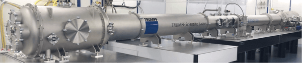
The 6-m-long Herriott cell for spectral broadening and subsequent pulse compression to <50 fs. TRUMPF confirmed that it is developing multiple secondary sources for different research projects funded by the German government. Courtesy of TRUMPF.
Zimer envisions laser modules with 5-kJ output of 20-ns pulses. Several hundred of these modules would be needed for a power station. “That would be a rugged and industrialized laser of about 10 m in length,” Zimer said. The entire topic will require participation from an international network, he said.
TRUMPF, meanwhile, will participate in a recently unveiled $42 million, DOE-funded research initiative aimed to continue to build momentum in the fusion arena. It is one of a growing number of companies, joining universities and R&D institutions, devoting expert-led work on laser components and systems to fusion. Further projects in Germany are looming.
Silicon photonics: Realizing the dream, or time to dream on?
Will silicon photonics (SiPh) boom anytime soon? What are the real prospects for PICs?
These questions are best addressed by a select few sector experts, including Roel Baets, founder of PIC advocacy group and European alliance ePIXfab. Baets, a former professor at Ghent University and imec, is a foremost authority and industry educator on SiPh.
In the OPTO conference plenary presentation, Baets delivered a seminal perspective on the near and more-distant future for PICs.
In a journey through many technical details, Baets showed where SiPh stands from a viewpoint that gave priority consideration to technology maturity. SiPh is related to and, indeed, often compared to semiconductor technologies. Will SiPh face the same business prospects? Backed by numbers from Yole Intelligence that indicate markets for SiPh may grow at a compound annual rate of 44% toward $3 billion in 2030, Baets himself estimates further growth — to $20 billion in 2040, or >1% of the market for regular semiconductors.
And yet, it is still something of a chicken-and-egg situation. And, perhaps, even something of a problem. To limit development and production costs, a “killer application” would go a long way in expediting the roadmap and boosting the financial figures that dot it. Though numerous fields develop relevant applications, each seeks simpler processes and lower costs. Telecom and datacom, for example, have already driven SiPh-based photonic solutions to great lengths.
Baets named promising fields for SiPh applications beyond transceiver products: biosensors; medical and industrial sensors; lidar and 3D imaging; higher performance interconnect and computing, such as AI and programmable; and quantum.
But many of these new applications require new functions or higher levels of performance; an important trend can achieve this through the addition of new materials. In short, more wavelengths, more optical power, more bandwidth, seamless integration with electronics, and new on-chip photonic functions are must-haves to push such applications forward. This prompts the question that heads this section. Baets sees SiPh as a dream for science: There is much to explore and ample fodder to support academic papers. But for industry, SiPh is also a “nightmare,” because of the diversity of process flows. The sheer number of materials needed is itself a headache, and some materials, such as lithium niobate (a fabulously efficient optical modulator material) permeate silicon to the point that an unwelcome arrival to the wrong fab could shutter operations.
Baets concluded his session with a set of recommendations. The need for standardization, continued use of existing and mature process flows — and new process flows designed to bypass major disruptions to existing flows — and calls for a robust PIC supply chain are at or near the top of these recommendations.
For those interested in the photonic solutions that are currently undergoing development, and where we stand in terms of manufacturability of the components needed, a paper from another group ought to serve as an introduction, authority, and, of course, roadmap for the present and future of SiPh1.
This too was remarkable
There is so much more to report. The country of Lithuania, for example, commanded the attention of the industry when Altechna acquired U.S.-based Alpine Research Optics in a transaction late last year. Two months later in San Francisco, the nation — a bona fide photonics powerhouse — promoted its new innovation hub in Silicon Valley.
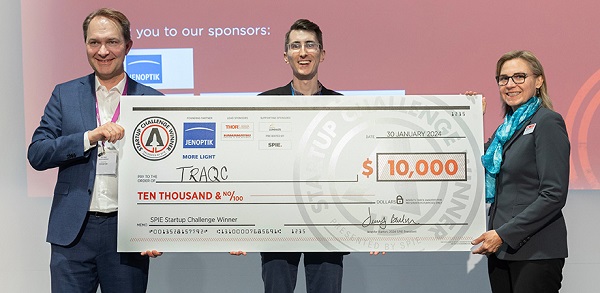
Benjamin Dringoli (center), cofounder and CEO of TRAQC, poses with Jenoptik executive Ralf Kuschnereit (left), and SPIE president Jennifer Barton after earning the top prize in the 2024 SPIE Startup Challenge. TRAQC develops nondestructive test technology for printed and additive electronics. Courtesy of SPIE.
And, of course, I must mention the progress reported in the quantum arena. To name just one example: Infleqtion claimed a world record 40 × 40 qubit array with neutral cesium atoms. The company plans to bring its gate fidelity to >99% by the end of this year while decoupling fidelity from qubit array scaling.
The photonics community will reconvene next year. Photonics West 2025 starts on Jan. 25, with the main exhibition following on Jan. 28.
See you then!
[email protected]
References
1. S. Shekhar et al. (January 2024). Roadmapping the next generation of silicon photonics. Nature Communications Vol. 15, Article number 751, www.doi.org/10.1038/s41467-024-44750-0.