Atom-based quantum devices rely on atom-photon interactions. Improving these interactions via integrated photonics will revolutionize atomic sensor designs.
JENNIFER T. CHOY UNIVERSITY OF WISCONSIN-MADISON
Measurements of isolated atomic systems have provided reliable means to standardize time and frequency, determine
fundamental constants with unprecedented
precision, and measure small electromagnetic fields and inertial forces. In particular, atomic measurements of time have
become ubiquitous and crucial in our daily life, from providing the base unit of time — the second currently being defined by the periodicity of electron oscillations in cesium atoms — to keeping time on board satellites in the global positioning system (GPS).
The ascendance of atomic technologies has been enabled by advancements in visible and near-infrared (NIR) photonics because preparation and measurement of atomic systems are typically performed via interactions with optical fields. For example, while the first atomic clocks used spectrally filtered discharge lamps, modern atomic sensors rely on NIR semiconductor lasers that can be tuned to or around atomic resonances of alkali atoms. The incorporation of lasers and other NIR photonic components has enabled the cooling of atoms, which has dramatically improved the performance of clocks and atomic inertial sensors and magnetometers, and enabled next-generation technologies such as quantum computing. Thus, improved performance in atomic devices can be derived from finer control of the frequency, phase, polarization, and direction of photons used to interact with atoms. At the same time, the push for device miniaturization imposes size requirements on photonic systems.
Atom-photon interactions
All quantum measurements involve the absorption and emission of electromagnetic radiation by quantized energy transitions. Transitions between atomic electron energy levels are especially appealing for precision measurements because atoms in a vacuum enclosure are isolated from the environment, behave independently and identically (if they are the same species), and have properties that do not change with time. In particular, alkali atoms such as rubidium (Rb) and cesium (Cs), which have one valence electron, are often used for atomic sensors because their electronic energy level structures are relatively simple (Figure 1). Interactions between the nucleus and valence electron lead to hyperfine states separated by megahertz to gigahertz microwave transitions, while NIR optical transitions arise from changes in electron orbital configurations. These transitions can also be affected by the presence of a magnetic field via the Zeeman effect, which is the basis for atomic magnetometry.
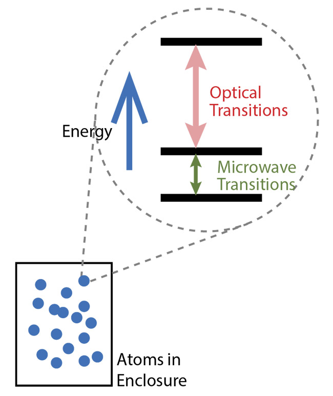
Figure 1. Energy transitions are found in the quantized degrees of freedom in isolated atoms, including microwave and optical transitions. Courtesy of J. Choy.
In a typical quantum-sensing measurement, atoms are prepared into a known initial state (for example, with all electrons occupying a particular hyperfine ground state) and are then allowed to interact with the environment. Then, a measurement of the post-interaction quantum state can be used to infer the physical quantities of interest (for example, magnetic or inertial fields) with high precision. These steps critically rely on atom-photon interactions that include the following:
Absorption and emission of photons by atoms (Figure 2a). Here, resonant light
excites atomic electrons to higher energy levels and is followed by spontaneous or stimulated emission. In spontaneous emission, excited electrons spontaneously decay to a lower energy level, emitting
fluorescence into a random direction.
Excited electrons can also return to the lower energy state via stimulated emission, in which the emitted photon is along the same direction of the absorbed photon. Photon absorption and stimulated emission are the processes by which electrons can be driven to coherently oscillate between energy levels.
Optical pumping (Figure 2b). Optical pumping refers to continuous, selective excitation of an optical transition to populate electrons in a preferential hyperfine state. After excitation, atomic electrons undergo spontaneous emission decay back to the pumped ground state (where they can be reexcited) as well as into one or more unpumped states. Over many pumping cycles,
electron population will accumulate in the unpumped state(s). Many optical pumping approaches rely on the conservation of angular momentum, which restricts whether a transition can be excited by a resonant photon based on the angular momentum it carries (which in turn is encoded in its polarization). Optical pumping provides an effective means to prepare a quantum system into an initial state and is especially crucial for polarizing atomic spins to maximize sensor signals in atomic magnetometers and gyroscopes.
Laser cooling (Figure 2c). Laser cooling utilizes momentum exchange between atoms and photons to reduce atomic motion. In the simplest configuration for laser cooling, an atom that is moving toward a laser (with the laser frequency tuned a bit lower than the atomic transition, to account for the Doppler shift experienced by the atom) absorbs an incoming photon and receives a momentum kick in the direction of the photon. The atom then undergoes spontaneous emission, with the scattered photon emitted in a random direction, resulting in a momentum kick in a random direction. After many such interactions, the net force counters the original atom motion, and the atom is thus slowed down. This technique, known as Doppler cooling, is commonly used to cool ensembles of atoms and can be combined with magnetic gradients to achieve trapping in a magneto-optical trap (MOT).
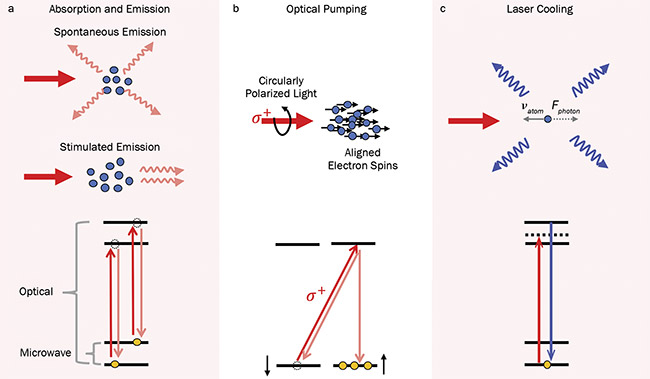
Figure 2.. Illustrations of major atom-photon interactions useful for atom-based sensing, along with the corresponding energy level diagrams: photon absorption and emission (a); use of circularly polarized light to optically pump atomic electrons into an electron spin state, thus effectively aligning all atomic spins along the same direction (b); laser cooling, in which an atom with velocity νatom absorbs a counter-propagating photon and undergoes spontaneous emission of a photon in a random direction. After many photon absorption-emission cycles, the resulting net force Fphoton counters the motion of the atom (c). Courtesy of J. Choy.
To illustrate how these interactions
underpin the operation of atomic sensors, various implementations of the atomic
clock are examined, one of which is shown in Figure 3.
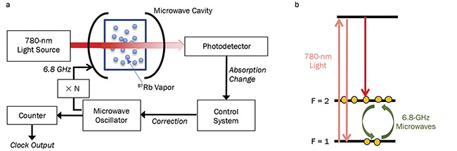
Figure 3. Operation of a rubidium vapor-cell clock (a). Relevant atomic transitions during clock operation (b). Courtesy of J. Choy.
How atomic clocks use photons
An atomic clock uses oscillations at an atomic transition frequency as a standard that is compared to the output of a reference oscillator, such as a quartz crystal. Because the properties of atoms are expected to be stable in the absence of environmental disturbances, the atomic transition frequency is expected to remain fixed. Therefore, any difference between the reference and atomic outputs is
attributed to an error in the reference
oscillator, which can then be corrected using a feedback loop. Typically this correction is done by changing the drive voltage or temperature of the oscillator. The actual output of an atomic clock is from counting the oscillations of the corrected reference oscillator, rather than the atomic oscillations.
In the implementation shown in Figure 3a, a 780-nm light source from a laser or discharge lamp passes through a glass cell containing 87Rb atomic vapor, a stable Rb isotope with ~6.8 GHz separating the two hyperfine ground states, and the transmitted power is then measured by a photodetector. The output frequency of the light source is tuned to selectively excite electrons from only the F = 1 hyperfine ground state, such that continuous excitation will populate electrons in the F = 2 state and deplete F = 1 electrons, until atoms in the vapor no longer absorb the light beam and most of the light reaches the detector. Resonant microwaves (at ~6.8 GHz) from a crystal oscillator are applied to atoms using a microwave cavity, causing population transfer between the hyperfine states. As the hyperfine populations reach equilibrium, the transmitted signal on the
photodiode will be minimized due to absorption by electrons that have repopulated F = 1. Changes to this transmission signal are then used in the clock’s control system to correct the crystal oscillator.
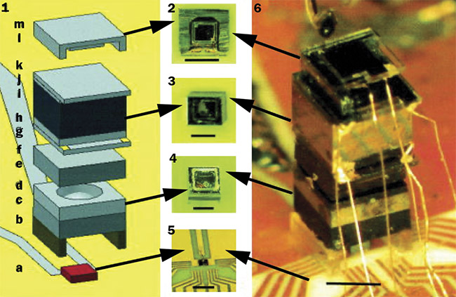
Figure 4. A chip-scale atomic clock, integrated with (from top to bottom) a photodiode, a Rb vapor cell made out of glass and silicon, lenses, filters, and a VCSEL. The scale bar (black line) in each subfigure indicates 1 mm and the entire package measures 4.2 × 1.5 × 1.5 mm3. Reprinted with permission from Reference 2. Courtesy of AIP Publishing.
Vapor-cell atomic clocks are a useful technology due to their relative simplicity and compatibility with microfabrication techniques, which have enabled chip-scale atomic clocks (Figure 4). (NIST researcher John Kitching authored a comprehensive review of microfabricated atomic clocks and magnetometers1.) However, a source of systematic error in chip-scale atomic clocks2 is the frequency drift arising from temperature changes in the atomic vapor that occur on the scale of hours. Clocks based on cold atoms prepared using laser cooling thus offer improved stability.
The primary time and frequency standard in the U.S. is based on a Cs cold-atom clock3 (NIST-F1, Figure 5) operated in a temperature- and vibration-controlled environment at NIST. This system uses three orthogonal pairs of counterpropagating, circularly polarized laser beams to cool and trap Cs atoms.
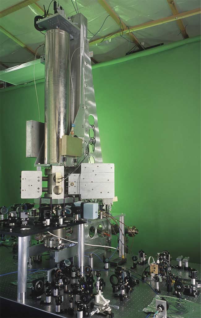
Figure 5. A photograph of the NIST-F1 cold Cs fountain clock located at NIST. The magnetically shielded region (nu-metal cylinder) is roughly 1 m in height. Courtesy of Geoffrey Wheeler.
Commercial atomic clocks, based on alkali metal vapor and cold-atom clocks such as the NIST-F1, all use the gigahertz hyperfine transitions of atoms, which can be compared to the outputs of megahertz-scale crystal oscillators using radio frequency (RF) multipliers. The final component of a clock is a counter for counting the number of oscillations, with the greater the number of oscillations within a fixed time window (higher frequency), the better the accuracy. Optical transitions in atoms would thus provide even more accurate timing, but they’re incompatible with standard frequency multiplication and counting electronics. In another example illustrating how advancements in photonic technologies can augment atomic-device performance, the development of optical frequency combs makes it possible to divide optical frequencies into the microwave domain, thus enabling optical clocks. While the NIST-F1 is accurate to a second in a 100 million years3, optical clocks are accurate to a fraction of a second in the lifetime of the universe (13.8 billion years)4. This level of accuracy would improve the many applications that currently rely on atomic clocks (timing, navigation, and communications), as well as enable fundamental physics experiments including gravitational wave detection.
Size and integration challenges
A comparison between vapor-cell and cold-atom clocks illustrates a common trade-off between atomic device performance (such as stability and accuracy) and size and complexity. Much of this trade-off can be attributed to the optical components needed to control atom-photon interactions. While the photonic design for a chip-scale atomic clock2 consists of only a vertical-cavity surface-emitting laser (VCSEL), lenses and filters, and a detector, more advanced clocks involving atom cooling require additional
components that greatly increase the
overall size and complexity, such as laser sources that can be frequency-tuned to different atomic transitions, amplitude modulators to generate light pulses, and passive optics (collimators, wave plates, and beam-steering optics) that control
the wavefront, direction, and polarization of light interacting with atoms.
Although the discussion thus far has focused on the atomic clock, the trade-off between performance and size can be even more challenging in other types of atomic sensors. For example, most atom-based
accelerometers and gyroscopes measure the deflection experienced by an ensemble of atoms (often cooled in a MOT) in the presence of motion, using a technique known as matter-wave or atom interferometry5. In this approach, optical pulses are used to coherently split and recombine the wave functions of atoms during their interaction with acceleration or rotational forces. The phase shift of the atom interferometer is measured via fluorescence detection and is used to infer the amount of acceleration or rotation. Atom interferometry is able to measure acceleration down to a precision of ~10−9 × Earth’s gravity, which makes it attractive for navigation applications and fundamental physics measurements such as tests of the equivalence between gravitational
and inertial mass. However, to achieve state-of-the-art accuracy and stability, atom interferometers require optical and electronic components that often take up an entire optical table, thus limiting the mobility of the sensor. Moreover, these optical setups are prone to optical-beam misalignments in response to thermal and mechanical changes in the environment, making sensor response more vulnerable to environmental disturbances.
Outlook: chip-scale integration
Techniques to miniaturize and better integrate optical setups would revolutionize atomic sensor designs and bring atomic sensing capabilities to their full potential. Prior efforts applying integrated photonics to atomic experiments have focused on cavity quantum electrodynamics, by coupling single atoms to high-quality-factor optical cavities, along with miniaturization of lasers such as VCSELs and fiber lasers. Recent progress has been made on compact atom trapping6 and interferometry architectures7 that use diffractive
gratings (Figure 6) or pyramidal mirrors, and photonic integrated vapor cells for atomic spectroscopy8. However, to achieve the vision of an all-integrated optical system for atomic sensors, further developments are needed in chip-scale components that provide active control and detection of photons (lasers, isolators, modulators, switches, and detectors), as well as efficient light delivery and polarization control (with waveguides, mode converters, and wave plates).
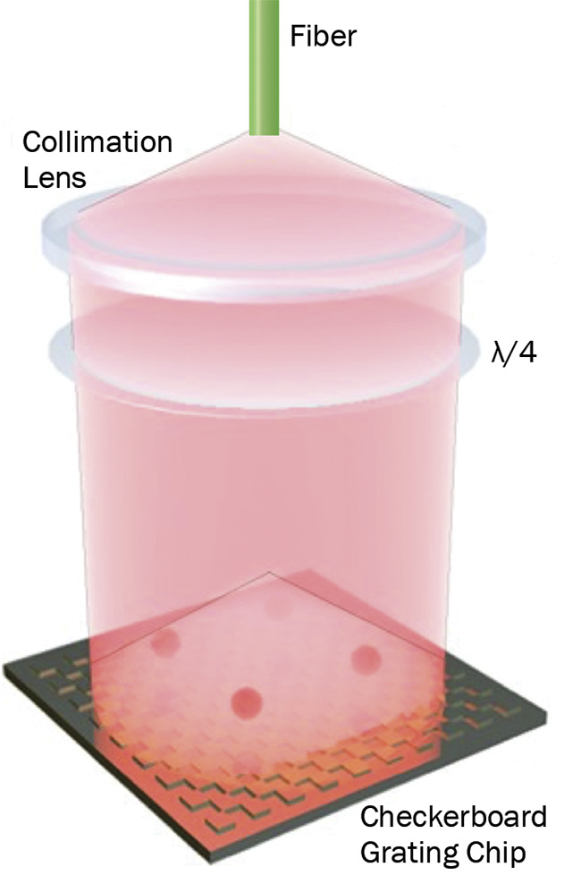
Figure 6. An illustration of a grating chip being used to cool and trap atoms. See Reference 6. Courtesy of Springer Nature.
In analogy to the size revolution in electronic circuits that came from integrating large numbers of transistors into an
integrated circuit, development of compact atomic sensors would require a paradigm shift away from relying on bulk, discrete components to an integrated photonics platform.
Meet the author
Jennifer T. Choy is an assistant professor of engineering physics at the University of
Wisconsin-Madison and was previously a scientist at Draper Laboratory. Her research interests include quantum sensing and nanophotonics; email: [email protected].
Acknowledgments
J. Choy gratefully acknowledges M. Kats for his critical reading and editing of this article, as well as funding support from the Office of Naval Research (N00014-20-1-2598).
References
1. J. Kitching (2018). Chip-scale atomic devices. Appl Phys Rev, Vol. 5, p. 031302.
2. S. Knappe et al. (2004). A microfabricated atomic clock. Appl Phys Lett, Vol. 85,
p. 1460.
3. T.P. Heavner et al. (2014). First accuracy evaluation of NIST-F2. Metrologia, Vol. 51, pp. 174-182.
4. T.L. Nicholson et al. (2015). Systematic evaluation of an atomic clock at 2 × 10⁻¹⁸ total uncertainty. Nat Commun, Vol. 6,
p. 6896.
5. M. Kasevich and S. Chu (1991). Atomic interferometry using stimulated Raman transitions. Phys Rev Lett, Vol. 67, p. 181.
6. J.P. McGilligan et al. (2017). Grating chips for quantum technologies. Sci Rep, Vol. 7, p. 384.
7. X. Wu et al. (2017). Multiaxis atom interferometry with a single-diode laser and a pyramidal magneto-optical trap. Optica, Vol. 4, pp. 1545-1551.
8. M.T. Hummon et al. (2018). Photonic chip for laser stabilization to an atomic vapor with 10−11 instability. Optica, Vol. 5,
pp. 443-449.