Silicon-based solar cells are the foundation of a variety of photovoltaic technologies and applications.
Casey Gutowski, Schott Solar Inc.
In the 1950s, scientists at Bell Labs serendipitously discovered that silicon doped with certain “impurities” is very sensitive to light. This discovery arrived just in time for the Space Age, when a source of electricity was needed for satellites and nearby solar system probes. Launched early in 1958, the first US satellite, Explorer I, was also the first spacecraft to use solar panels.
Today, silicon-based photovoltaic cells are integrated into consumer products such as calculators and garden lighting to provide electricity without the need for batteries or a power cord. And increasingly, homeowners, corporations and government agencies are using silicon-based photovoltaic cells to generate electricity for their own use or to feed into the grid.
New materials such as gallium arsenide and indium selenide are used to produce solar cells, but silicon is the material of choice for photovoltaic applications worldwide. This is because the raw material from which it is made (sand) is plentiful, and it is nontoxic — a key advantage given that environmental protection is one of the major reasons behind the move toward solar energy — and its optoelectrical properties are well-established and are constantly being refined.
Facilities for purifying silicon to the levels required for photovoltaic applications already have been developed for the computer industry and can be rapidly expanded. Its chemical stability enables it to work for decades. And because silicon solar cells can function in temperatures up to 125 °C, they can withstand the most extreme weather conditions on Earth. The Renewable Energy Policy Network for the 21st Century, a global network that provides a forum for international leadership on renewable energy, estimates that grid-connected solar photovoltaic capacity is increasing from 3.5 GW in 2005 to an estimated 7.8 GW in 2008.
Silicon is an excellent material for generating electricity, but it does pose certain challenges. Although it is abundant as a raw material, a highly refined and lengthy process is required to produce solar-grade silicon. The semiconductor industry has increased worldwide demand for silicon in general, but silicon refineries have failed, until recently, to invest in the infrastructure needed to produce solar-grade silicon. Today many silicon refiners are establishing joint ventures or are signing long-term contracts with photovoltaic manufacturers, helping to ensure a stable supply of silicon to the photovoltaic industry.
Silicon photovoltaic technologies
There are several ways to make silicon photovoltaic cells, including single-crystal, or monocrystalline, silicon, multicrystalline silicon, ribbon silicon and amorphous thin-film silicon. For the monocrystalline type, the basic manufacturing method is the Czochralski process, in which solid cylindrical boules or ingots of single-crystal silicon are grown. Each boule is typically 400 mm in diameter and 1 or 2 m long. To make the silicon, n-type or p-type dopants are added during the process. Monocrystalline silicon photovoltaic cells have the best energy conversion rates of any silicon photovoltaic technology (Table 1).
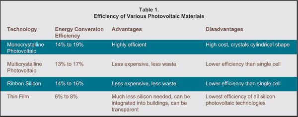
Table 1. Shown is the efficiency of various photovoltaic materials, ranging from monocrystalline silicon to thin film. Source: PV Technology, Performance, and Cost — 2007 Update, Prometheus Institute for Sustainable Development.
Growing single crystals consumes much time and energy when compared with other methods, making monocrystalline silicon growth and finishing relatively expensive. In addition, when the crystals are grown, the photovoltaic components must be cut from cylindrical ingots. The resulting circular shapes do not match the standard square cell module. Although cutting can solve this problem, it also creates a lot of waste. As an alternative, circular slices of the crystal can be attached to square solar cell modules, leaving gaps at all four corners. Here the price is paid in efficiency. These drawbacks notwithstanding, the vast majority of silicon photovoltaic cells are produced using a monocrystalline process.
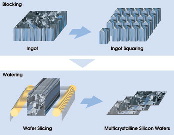
Figure 1. A new technique in the production of multicrystalline photovoltaic cells uses a laser to cut wafers out of the surface of a hollow edge-defined film-fed growth tube.
In multicrystalline silicon, molten silicon is poured into a large molding container and then carefully cooled and solidified. The cells start out as cast square ingots, so when sliced into wafers, they readily fit the solar cells (Figure 1). Several photovoltaic manufacturers have developed techniques that reduce the material waste in this process. For example, Schott Solar has patented the EFG process, which eliminates the saws and reduces waste in the production of multicrystalline photovoltaic cells. In this process, a silicon film in the form of an octagonal hollow tube is pulled directly from the silicon melt, and a laser cuts out the wafers, thereby reducing waste (Figure 2).
Figure 2. Cast square ingots are sliced into wafers, ready to fit on solar cells.
Multicrystalline cells are less expensive to produce than single-crystal cells, and the finished product produces relatively efficient energy conversion of between 13 and 17 percent — good, but not quite as good as single-crystal cells.
Trends in the multicrystalline technologies have focused on increasing the efficiency of the modules. One way to achieve this is by adding more usable surface area. For example, Schott Solar recently announced a process that can increase a cell’s surface area. This wet chemical process “roughens” the surface of a cell. By creating peaks and valleys, the cell — in addition to having lateral surface area — now also has a vertical depth, increasing its usable size.
Ribbon silicon is fabricated using a variety of solidification (crystallization) methods that withdraw flat, thin silicon sheets or films from pools of relatively pure molten silicon. Ribbon silicon features a multicrystalline structure and offers lower production costs and less waste than monocrystalline production. With the silicon in thin ribbons, most of the energy used to slice the wafers in the single- and multicrystal processes is eliminated. Moreover, the ribbons can be stretched to the desired thickness. However, ribbon silicon cells, with efficiency conversion ratings of 14 to 16 percent, are generally less efficient than monocrystalline photovoltaic cells and do not offer as strong an efficiency rating on the high end as regular multicrystalline cells.
Thin-film devices
Amorphous thin-film silicon has physical properties similar to those of glass, making it more fluidlike than comparatively rigid crystalline silicon. To make a thin-film panel, a conductive metal such as an indium oxide/tin oxide mix is deposited onto a piece of glass. Three silicon layers come next, each about 20-millionth of an inch thick. These are applied by stimulating silicon plasma with radio frequency bombardment until it breathes a layer of p-type semiconductor silicon onto the transparent conductive oxide layer. An insulator of undoped (nonconductive) silicon goes next, followed by another layer of p-type semiconductor silicon. The negative contact is provided by a covering of nickel vanadium.
One of amorphous thin film’s advantages is that it integrates easily into buildings and other structures. Although photovoltaic panels are traditionally add-ons, thin-film modules can be encapsulated in glass that is framed and then integrated into curtain walls, skylights or rooftops. Through laser etching, thin-film panels also can become semi-transparent to allow in natural day lighting. This also can reduce the energy needed to heat a given structure. However, etching the module does reduce the usable surface area for generating electricity.
Another advantage of thin film is that it uses one-fiftieth of the silicon required for conventional solar cells. There is also less waste than there is with mono- and multicrystalline panels and fewer production steps. Unfortunately, the cells themselves have efficiency ratings of 6 to 8 percent. Because of this, more thin-film modules are needed to produce the same amount of power. Many photovoltaic companies are working to improve thin film’s efficiency and to make it a more attractive photovoltaic alternative.
The largest building-integrated thin-film solar installation in the US is at the Stillwell Avenue subway station at Coney Island, N.Y., where a roof consisting of 2800 thin-film modules covers a surface of 76,000 square feet (7100 m2). This installation has a capacity 210 kW peak and generates approximately 250,000 kWh of electricity per year (Figure 3).

Figure 3. The roof of the Stillwell Avenue train station in New York is home to the largest building-integrated solar plant with thin-film modules in the US.
Alternatives to silicon
Cells made of relatively exotic materials such as gallium arsenide or iridium selenide can be more efficient than silicon cells but are more expensive to produce. These substances are a long way from deployment on rooftops or in utility-scale solar power arrays. In fairness to the exotics, it should be noted that gallium arsenide is being used to power the Mars rovers, which have been exploring Mars for about two years after their “expiration date.” This technology has proved itself in the dusty and thin Mars atmosphere. Still, here on Earth we expect panels to work for 30 years and to endure heavier weather than the atmosphere of Mars can throw at a solar cell.
Organic photovoltaics, built around carbon instead of silicon, also have been developed from polymers, but their critical weakness is that they are easily degraded by UV light. Also, unlike silicon cells, which work with the full array of light, organics tend to absorb only about a third of the spectrum of visible light. Still, they offer promise because they can be produced in very thin, lightweight and even transparent layers and have the potential to work with the IR portion of the solar spectrum.
Barring major technological leaps in the development of silicon photovoltaic alternatives, it seems clear that the early part of this century’s large-scale solar electricity generation infrastructure will be built on the foundation of silicon photovoltaic cells. There are several technical and economic advantages, and many of the manufacturing and production problems have been solved. Moreover, expanding silicon solar photovoltaic panel production should be no more complicated than the vast expansion of semiconductor production in the last quarter of the 20th century — just on a greater scale, and possibly in service to a more important goal.
Meet the author
Casey Gutowski is director of business development and policy at Schott Solar in Roseville, Calif.; e-mail: [email protected].